15
ATtiny26(L)
1477G–AVR–03/05
Memories The AVR CPU is driven by the System Clock Ø, directly generated from the external
clock crystal for the chip. No internal clock division is used.
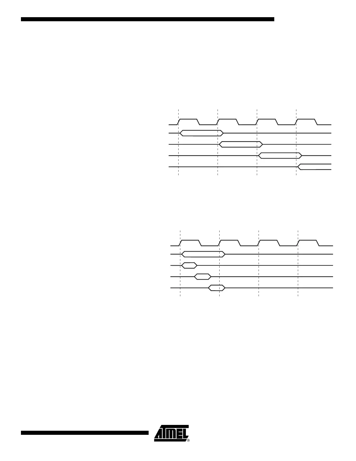
Figure 16 shows the parallel instruction fetches and instruction executions enabled by
the Harvard architecture and the fast-access Register File concept. This is the basic
pipelining concept to obtain up to 1 MIPS per MHz with the corresponding unique results
for functions per cost, functions per clocks, and functions per power-unit.
Figure 16. The Parallel Instruction Fetches and Instruction Executions
Figure 17 shows the internal timing concept for the Register File. In a single clock cycle
an ALU operation using two register operands is executed, and the result is stored back
to the destination register.
Figure 17. Single Cycle ALU Operation
The internal data SRAM access is performed in two System Clock cycles as described
in Figure 18.
System Clock Ø
1st Instruction Fetch
1st Instruction Execute
2nd Instruction Fetch
nd Instruction Execute
3rd Instruction Fetch
3rd Instruction Execute
4th Instruction Fetch
System Clock Ø
Total Execution Time
egister Operands Fetch
ALU Operation Execute
Result Write Back