91
ATtiny26(L)
1477G–AVR–03/05
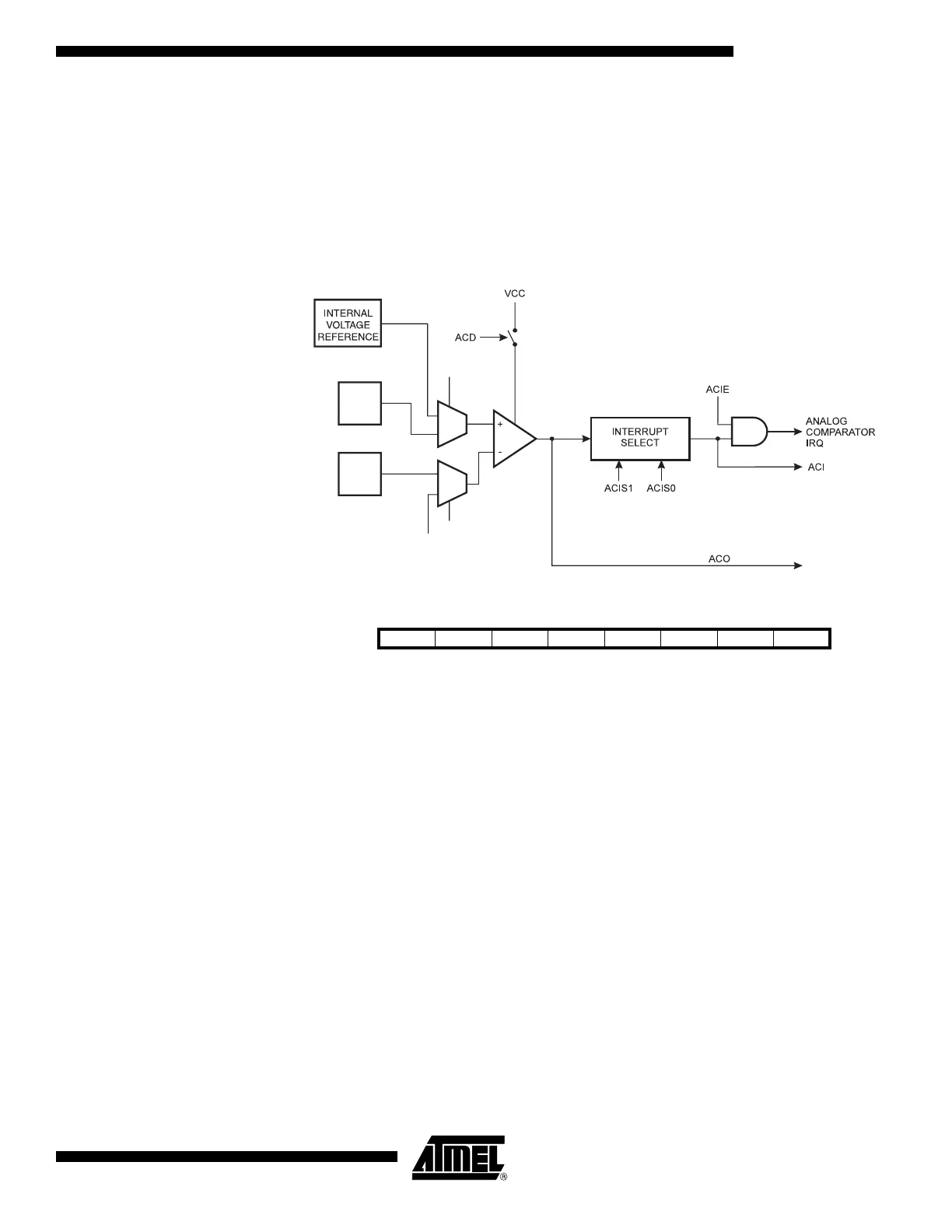
Analog Comparator The Analog Comparator compares the input values on the positive pin PA6 (AIN0) and
negative pin PA7 (AIN1). When the voltage on the positive pin PA6 (AIN0) is higher than
the voltage on the negative pin PA7 (AIN1), the Analog Comparator Output, ACO is set
(one). The comparator’s output can trigger a separate interrupt, exclusive to the Analog
Comparator. The user can select Interrupt triggering on comparator output rise, fall or
toggle. A block diagram of the comparator and its surrounding logic is shown in the Fig-
ure 50.
Figure 50. Analog Comparator Block Diagram
Analog Comparator Control
and Status Register – ACSR
• Bit 7 – ACD: Analog Comparator Disable
When this bit is set(one), the power to the Analog Comparator is switched off. This bit
can be set at any time to turn off the Analog Comparator. When changing the ACD bit,
the Analog Comparator Interrupt must be disabled by clearing the ACIE bit in ACSR.
Otherwise an interrupt can occur when the bit is changed.
• Bit 6 – ACBG: Analog Comparator Bandgap Select
When this bit is set (one), it selects internal bandgap reference voltage (1.18V) as the
positive comparator input.
• Bit 5 – ACO: Analog Comparator Output
ACO is directly connected to the comparator output.
PA6
(AIN0)
PA7
MUX
MUX
MUX
ADC
MULTIPLEXER OUTPUT
(AIN1)
ACBG
ACME
Bit 76543210
$08 ($28) ACD ACBG ACO ACI ACIE ACME ACIS1 ACIS0 ACSR
Read/Write R/W R/W R R/W R/W R/W R/W R/W
Initial Value 0 0 X 0 0 0 0 0