EasyManua.ls Logo

Atmel ATtiny26 User Manual

Atmel ATtiny26
182 pages
To Next Page IconTo Next Page
To Previous Page IconTo Previous Page
Page #7 background image
7
ATtiny26(L)
1477G–AVR–03/05
The AVR uses a Harvard architecture concept with separate memories and buses for
program and data memories. The program memory is accessed with a two stage
pipelining. While one instruction is being executed, the next instruction is pre-fetched
from the program memory. This concept enables instructions to be executed in every
clock cycle. The program memory is In-System programmable Flash memory.
With the relative jump and relative call instructions, the whole address space is directly
accessed. All AVR instructions have a single 16-bit word format, meaning that every
program memory address contains a single 16-bit instruction.
During interrupts and subroutine calls, the return address program counter (PC) is
stored on the Stack. The Stack is effectively allocated in the general data SRAM, and
consequently the stack size is only limited by the total SRAM size and the usage of the
SRAM. All user programs must initialize the SP in the reset routine (before subroutines
or interrupts are executed). The 8-bit Stack Pointer SP is read/write accessible in the I/O
space. For programs written in C, the stack size must be declared in the linker file. Refer
to the C user guide for more information.
The 128 bytes data SRAM can be easily accessed through the five different addressing
modes supported in the AVR architecture.
The memory spaces in the AVR architecture are all linear and regular memory maps.
The I/O memory space contains 64 addresses for CPU peripheral functions as Control
Registers, Timer/Counters, and other I/O functions. The memory spaces in the AVR
architecture are all linear and regular memory maps.
A flexible interrupt module has its control registers in the I/O space with an additional
Global Interrupt Enable bit in the Status Register. All the different interrupts have a sep-
arate Interrupt Vector in the Interrupt Vector table at the beginning of the program
memory. The different interrupts have priority in accordance with their Interrupt Vector
position. The lower the Interrupt Vector address, the higher the priority.
General Purpose
Register File
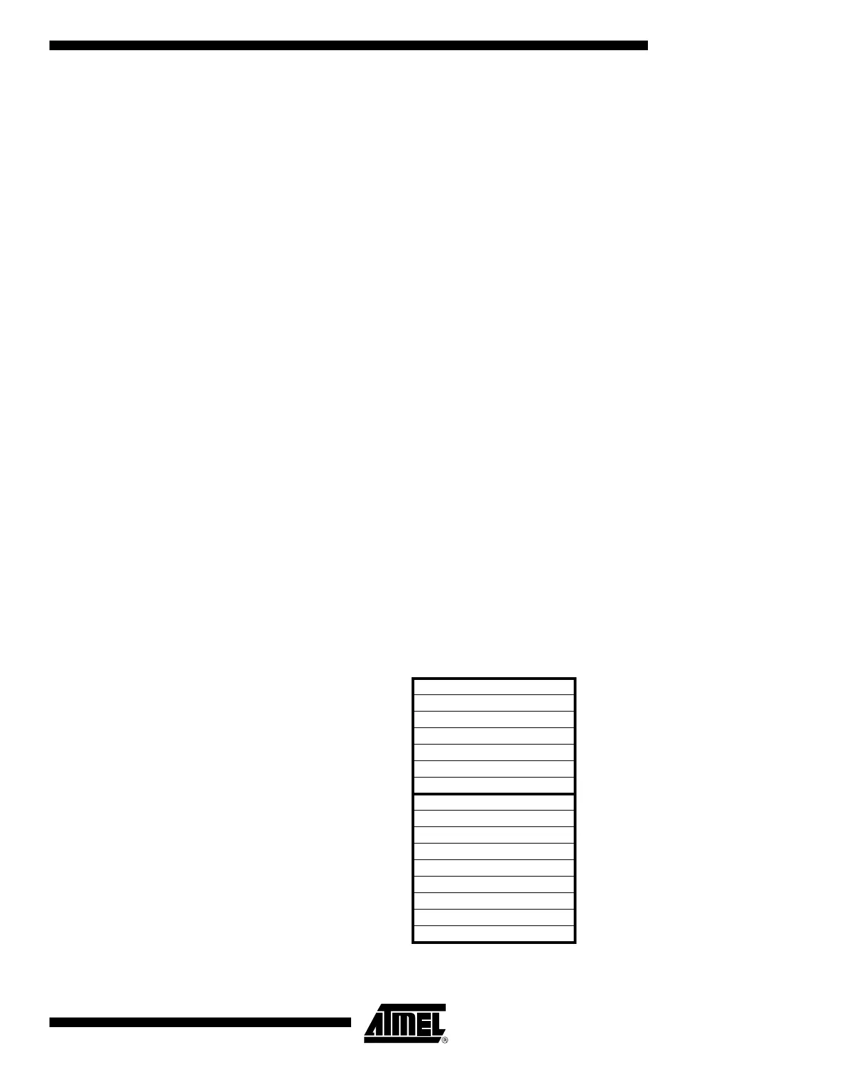
Figure 3 shows the structure of the 32 general purpose working registers in the CPU.
Figure 3. AVR CPU General Purpose Working Registers
7 0 Addr.
R0 $00
R1 $01
R2 $02
R13 $0D
General R14 $0E
Purpose R15 $0F
Working R16 $10
Registers R17 $11
R26 $1A X-register Low Byte
R27 $1B X-register High Byte
R28 $1C Y-register Low Byte
R29 $1D Y-register High Byte
R30 $1E Z-register Low Byte
R31 $1F Z-register High Byte

Table of Contents

Question and Answer IconNeed help?

Do you have a question about the Atmel ATtiny26 and is the answer not in the manual?

Atmel ATtiny26 Specifications

General IconGeneral
BrandAtmel
ModelATtiny26
CategoryMicrocontrollers
LanguageEnglish

Summary

Features

High-performance, Low-power AVR0 8-bit Microcontroller

High-performance, low-power 8-bit AVR microcontroller with RISC architecture.

RISC Architecture

Describes the RISC architecture of the ATtiny26(L) microcontroller.

Data and Non-volatile Program Memory

Details the Flash, EEPROM, and SRAM memory specifications.

Peripheral Features

Lists peripheral features like Timers, ADC, Comparator.

Special Microcontroller Features

Highlights features like low power modes, reset, interrupts.

Operating Voltages

Defines the operating voltage ranges for ATtiny26L and ATtiny26.

Speed Grades

Specifies the operating speed ranges for ATtiny26L and ATtiny26.

Power Consumption

Details power consumption in active and idle modes.

Pin Configuration

Description

Block Diagram

Pin Descriptions

Port A (PA7..PA0)

Describes Port A as an 8-bit general purpose I/O port with alternate functions.

Port B (PB7..PB0)

Describes Port B as an 8-bit general purpose I/O port with alternate functions.

AVR CPU Core

Architectural Overview

Explains the AVR RISC architecture and register file concept.

Status Register 0 SREG

Stack Pointer 0 SP

Program and Data Addressing Modes

Register Direct, Two Registers Rd and Rr

Details direct register addressing for two registers.

I/O Direct

Explains direct addressing for I/O memory locations.

Data Indirect with Displacement

Describes indirect addressing with displacement calculation.

Data Indirect with Pre-decrement

Explains indirect addressing with pre-decrement operation.

Data Indirect with Post-increment

Details indirect addressing with post-increment operation.

Indirect Program Addressing, IJMP and ICALL

Covers indirect addressing for program memory jumps and calls.

Memories

In-System Programmable Flash Program Memory

Details the 2K byte in-system programmable Flash memory for program storage.

SRAM Data Memory

Describes the 128 bytes of internal SRAM organization and usage.

EEPROM Data Memory

Covers the 128 bytes of EEPROM memory, organization, and read/write access.

System Clock and Clock Options

Clock Sources

Lists selectable clock source options via Flash Fuse bits.

Crystal Oscillator

External RC Oscillator

Calibrated Internal RC Oscillator

External Clock

High Frequency PLL Clock 0 PLLCLK

System Control and Reset

Power-on Reset

Details the on-chip detection circuit for power-on reset generation.

External Reset

Explains how to generate an external reset via the RESET pin.

Brown-out Detection

Describes the on-chip BOD circuit for monitoring VCC level during operation.

Power Management and Sleep Modes

MCU Control Register 0 MCUCR

Contains control bits for general MCU functions, including sleep modes.

Idle Mode

Stops CPU, allows peripherals to run; halts clkCPU and clkFLASH.

ADC Noise Reduction Mode

Halts clkIO, clkCPU, clkFLASH; improves ADC noise environment.

Power-down Mode

Stops external oscillator; halts most clocks, allows async modules to run.

Standby Mode

Similar to power-down, but keeps the oscillator running.

I/O Ports

Ports as General Digital I/O

Describes bi-directional I/O ports with optional internal pull-ups.

Alternate Port Functions

Details alternate functions for port pins beyond general digital I/O.

Interrupts

Interrupt Vectors

Lists interrupt sources, program vectors, and priority levels.

Interrupt Handling

Explains interrupt occurrence, disabling, and response time.

External Interrupt

Pin Change Interrupt

Timer/Counters

8-bit Timer/Counter0

Details the 8-bit Timer/Counter0, its block diagram, and control registers.

8-bit Timer/Counter1

Covers Timer/Counter1 modes, prescalers, and PWM capabilities.

Watchdog Timer

Universal Serial Interface 0 USI

Register Descriptions

Describes USI data register, status register, and control register.

Functional Descriptions

Explains three-wire and two-wire modes, and alternative USI usages.

Analog Comparator

Analog to Digital Converter

Features

Lists key features of the 10-bit successive approximation ADC.

ADC Conversion Result

Explains how to find and interpret the ADC conversion result.

Memory Programming

Program and Data Memory Lock Bits

Details lock bits for protecting Flash and EEPROM programming.

Fuse Bits

Signature Bytes

Calibration Byte

Page Size

Parallel Programming Parameters, Pin Mapping, and Commands

Parallel Programming

Describes the algorithm to put the device into parallel programming mode.

Serial Downloading

Explains programming via the serial SPI bus interface.

Electrical Characteristics

Absolute Maximum Ratings*

Lists the stress limits beyond which damage may occur to the device.

DC Characteristics

Provides DC electrical parameters like voltage thresholds and currents.

ADC Characteristics

Details ADC performance metrics for single-ended and differential channels.

ATtiny26 Typical Characteristics

Register Summary

Instruction Set Summary

Ordering Information

Packaging Information

20P3

Details the 20-lead PDIP package dimensions and specifications.

20S

Details the 20-lead SOIC package dimensions and specifications.

32M1-A

Details the 32-pad MLF package dimensions and specifications.

Errata

Datasheet Revision History

Related product manuals