44
ATtiny26(L)
1477G–AVR–03/05
signal transition on the pin will be delayed between ½ and 1½ system clock period
depending upon the time of assertion.
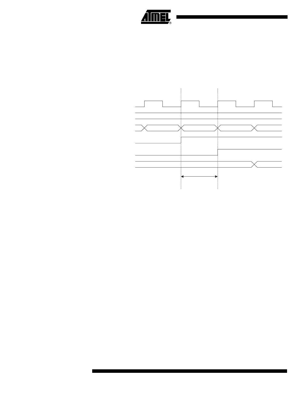
When reading back a software assigned pin value, a nop instruction must be inserted as
indicated in Figure 34. The out instruction sets the “SYNC LATCH” signal at the positive
edge of the clock. In this case, the delay t
pd
through the synchronizer is one system
clock period.
Figure 34. Synchronization when Reading a Software Assigned Pin Value
out PORTx, r16 nop in r17, PINx
0xFF
0x00 0xFF
SYSTEM CLK
r16
INSTRUCTIONS
SYNC LATCH
PINxn
r17
t
pd