66
ATtiny26(L)
1477G–AVR–03/05
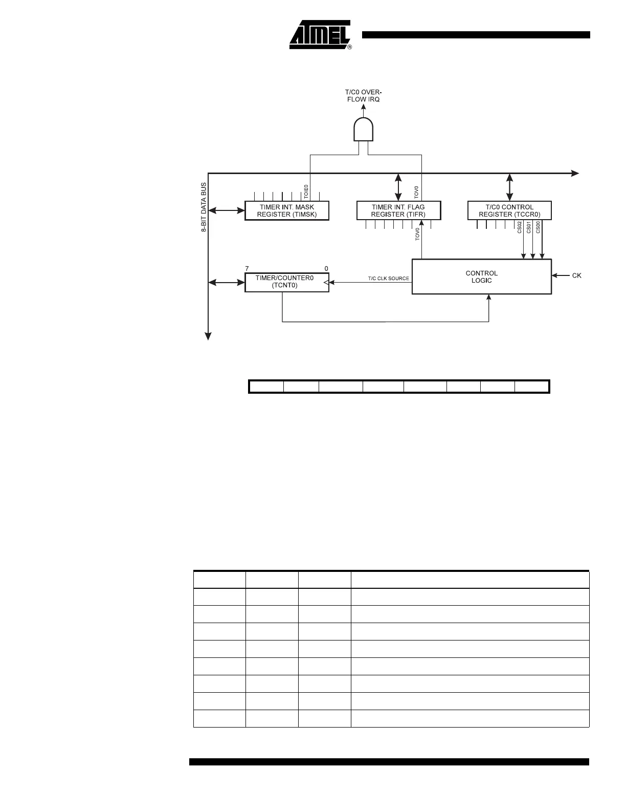
Figure 38. Timer/Counter0 Block Diagram
Timer/Counter0 Control
Register – TCCR0
• Bits 7..4 – Res: Reserved Bits
These bits are reserved bits in the ATtiny26(L) and always read as zero.
• Bit 3 – PSR0: Prescaler Reset Timer/Counter0
When this bit is set (one), the prescaler of the Timer/Counter0 will be reset. The bit will
be cleared by hardware after the operation is performed. Writing a zero to this bit will
have no effect. This bit will always be read as zero.
• Bits 2, 1, 0 – CS02, CS01, CS00: Clock Select0, Bit 2, 1, and 0
The Clock Select0 bits 2, 1, and 0 define the prescaling source of Timer0.
Bit 76 5 4 3 210
$33 ($53) – – – – PSR0 CS02 CS01 CS00 TCCR0
Read/Write R R R R R/W R/W R/W R/W
Initial Value 0 0 0 0 0 0 0 0
Table 31. Clock 0 Prescale Select
CS02 CS01 CS00 Description
0 0 0 Stop, the Timer/Counter0 is stopped
001CK
010CK/8
011CK/64
100CK/256
101CK/1024
1 1 0 External Pin T0, falling edge
1 1 1 External Pin T0, rising edge