88
ATtiny26(L)
1477G–AVR–03/05
the master device, and when the transfer is completed the data received from the mas-
ter is stored back into the r16 register.
Note that the first two instructions is for initialization only and needs only to be executed
once.These instructions sets Three-wire mode and positive edge Shift Register clock.
The loop is repeated until the USI Counter Overflow Flag is set.
Two-wire Mode The USI Two-wire mode is compliant to the Inter IC (TWI) bus protocol, but without slew
rate limiting on outputs and input noise filtering. Pin names used by this mode are SCL
and SDA.
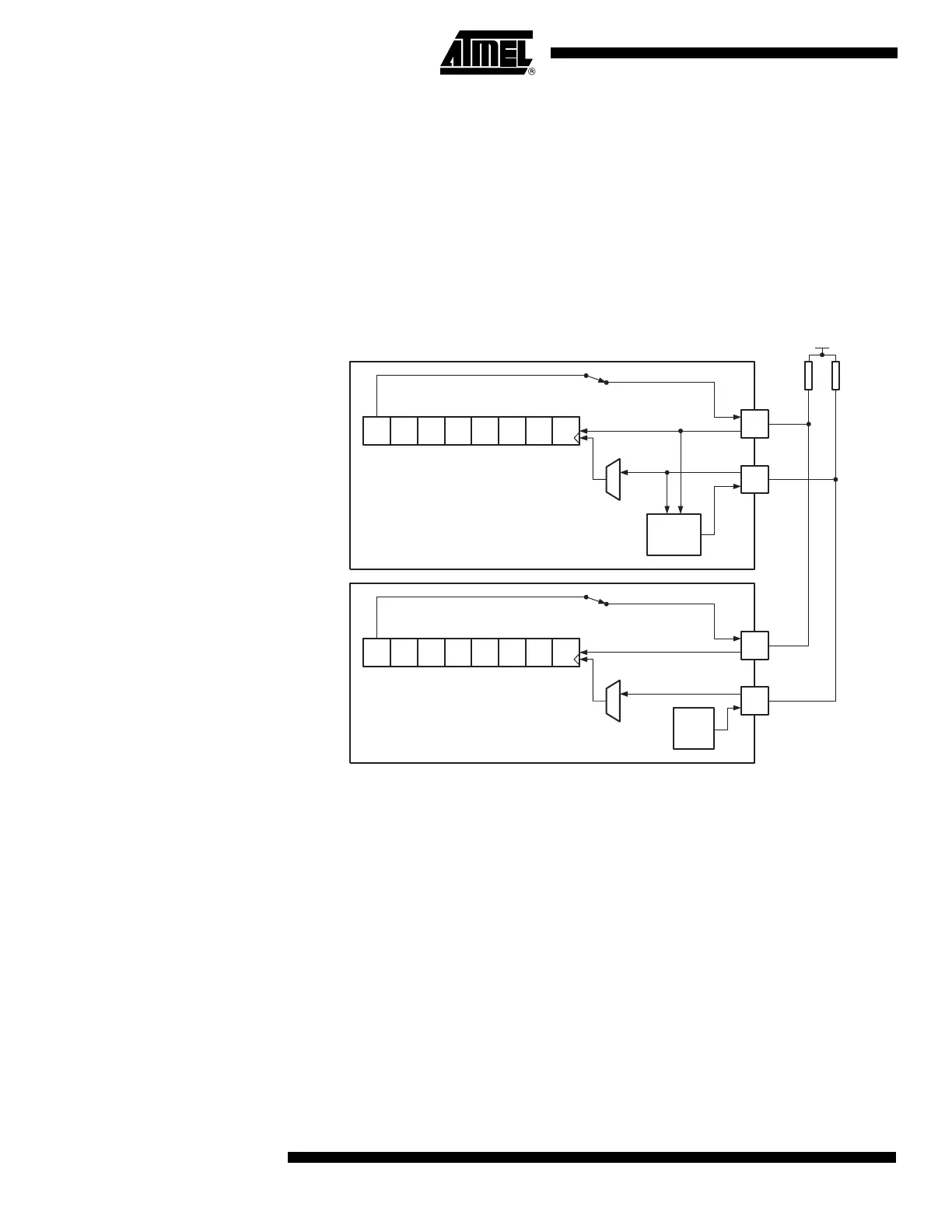
Figure 47. Two-wire Mode Operation, Simplified Diagram
Figure 47 shows two USI units operating in Two-wire mode, one as master and one as
slave. It is only the physical layer that is shown since the system operation is highly
dependent of the communication scheme used. The main differences between the mas-
ter and slave operation at this level, is the serial clock generation which is always done
by the master, and only the slave uses the clock control unit. Clock generation must be
implemented in software, but the shift operation is done automatically by both devices.
Note that only clocking on negative edge for shifting data is of practical use in this mode.
The slave can insert wait states at start or end of transfer by forcing the SCL clock low.
This means that the master must always check if the SCL line was actually released
after it has generated a positive edge.
Since the clock also increments the counter, a counter overflow can be used to indicate
that the transfer is completed. The clock is generated by the master by toggling the PB2
pin via the PORTB Register.
The data direction is not given by the physical layer. A protocol, like the one used by the
TWI-bus, must be implemented to control the data flow.
MASTER
SLAVE
Bit7 Bit6 Bit5 Bit4 Bit3 Bit2 Bit1 Bit0
PBy
PBz
SDA
SCL
Bit7 Bit6 Bit5 Bit4 Bit3 Bit2 Bit1 Bit0
Two-wire Clock
Control Unit
PBy
PBz
HOLD
SCL
PORTBz
SDA
SCL
VCC