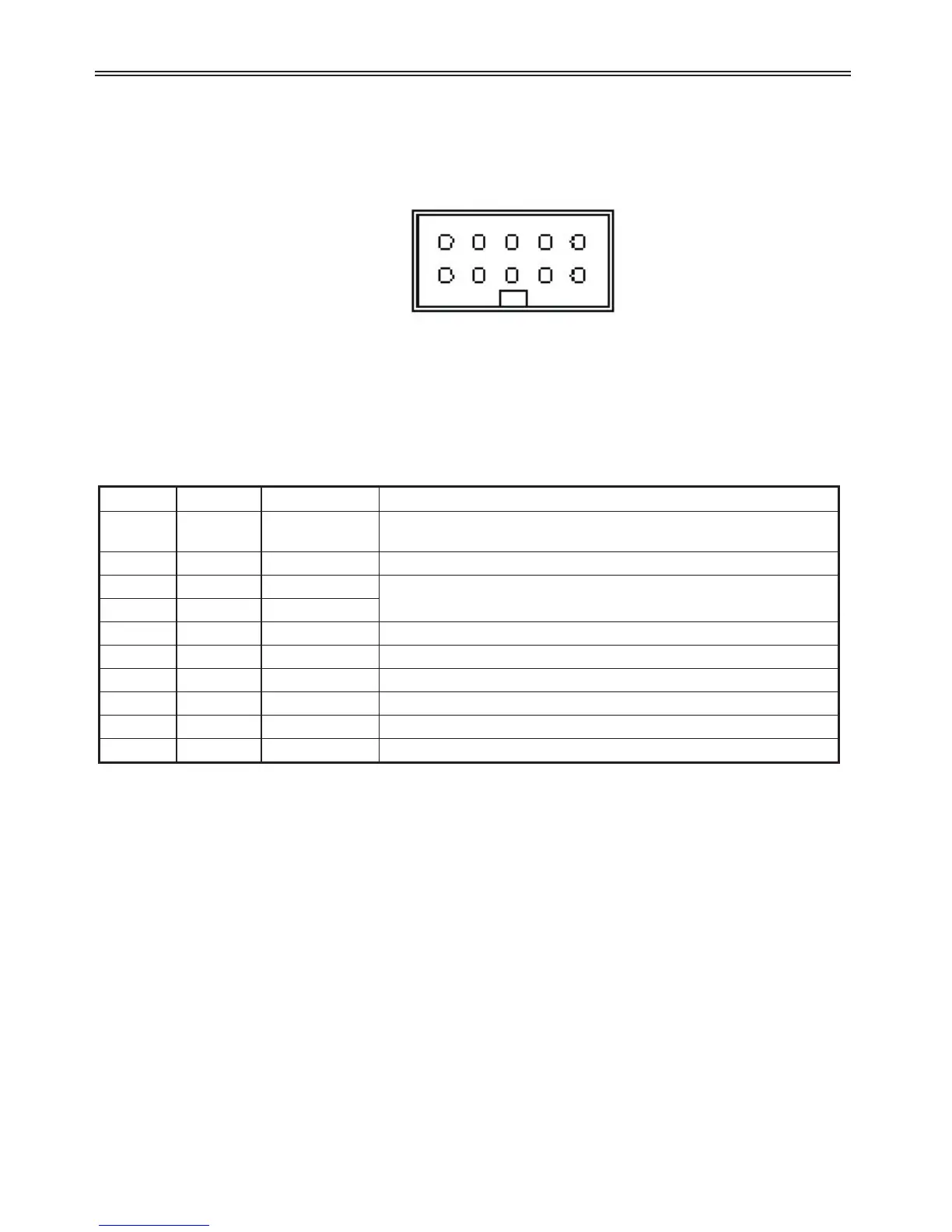
Keypad Connector Pin Configuration (Drive side)
34
3 - RECEIVING AND INSTALLATION
Pin No. Pin Name Keypad Description
1 5V Used
5V DC power supply (Isolated from VR, V1, I of control
terminal)
2 GND Used 5V DC power ground (Isolated from CM of control terminal)
3 RES Used
Used for writing the flash ROM inside drive.
4 VPP Used
5 LAT Used Latch signal for transmitting/receiving
6 TXD Used Transmitting signal pin
7 CLK Used Clock signal pin
8 RXD Used Receiving signal pin
9 Not Used
10 Not Used
2
1
3
5
7
9
4
6
8
10
(Top View)
 Loading...