DSB75 Development Support Board Rev. B1 Hardware Description
Confidential / Released
DSB75_hd_v12 Page 28 of 96 2008-08-26
S110
X510
X511
S501
S500
S457
S452
S456S455
S453
S454
S450
S460
S451
S461 S462
S464S4 65
S463
S466
S4 69
S459
S467
S458
S468
V450
V451
V452
V453
V457
V456
V504
V503
V455
V454
V
2
3
7
V
2
3
2
V
2
3
6
V
2
3
1
V
2
3
5
V
2
3
0
V
2
3
4
V
2
4
4
V
2
4
3
V
2
4
2
V
2
4
1
V
2
3
9
V
2
4
0
V
2
3
8
V
2
3
3
SD_D0 (GPIO1)
SD_D1 (GPIO2)
SD_D2 (GPIO3)
SD_D3 (GPIO4)
SD_CLK (GPIO5)
SD_CMD (GPIO6)
R
X
D
2
_
G
P
I
O
9
T
X
2
_
G
P
I
O
1
0
I2CDAT
I2CCLK
2
1
1
0
1
2
1
0
1
3
9
9
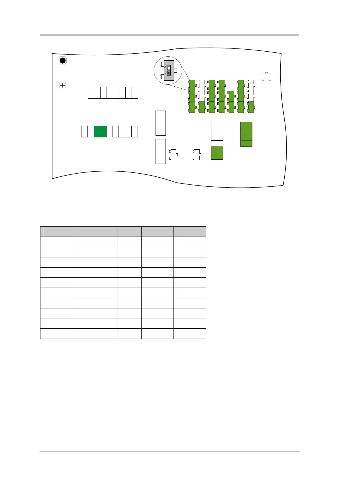
Figure 8: GPIO - location of switches and LEDs
Table 9: GPIO assignment and switch position
X100 pin Signal name GPIO S450-459 S460-469
71 SD_D0 1 S450:3 S460:x
1
72 SD_D1 2 S451:3 S461:x
73 SD_D2 3 S452:3 S462:x
74 SD_D3 4 S453:3 S463:x
10 SD_CLK 5 S454:3 S464:x
9 SD_CMD 6 S455:3 S465:x
8 SD_DET 7
6 SD_WP 8
76 RXD2_GPIO9 9 S458:3 S468:x
5 TXD2_GPIO10 10 S459:3 S469:x
1
Switch position x may be position 1 or 3.
high level input: x=1
low level input: x=3
Electrical characteristics are specified in section
8.