DSB75 Development Support Board Rev. B1 Hardware Description
Confidential / Released
DSB75_hd_v12 Page 60 of 96 2008-08-26
3.14.1 Internal Supply Voltages
This section describes the internal supply voltages generated by the power supply unit of
DSB75. A simplified block diagram of the power supply concept is shown in section
3.14.
Table 25: Description of power supply units
Power Supply Unit Description
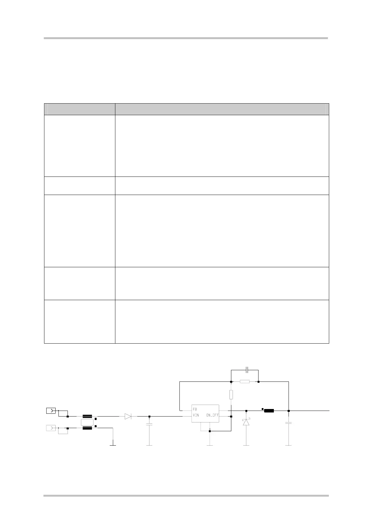
General supply 5V0
(see
Figure 34)
DSB75 accepts an input voltage between 9V and 15V DC on jacks X400
and X401.
These ports are protected against polarity reversal by a simple diode V400.
To reduce power dissipation, a DC/DC converter N400 provides a constant
voltage of 5.0V. This voltage is used for supplying 3 LDOs and the audio
section with power and is available for battery charging, supplying I2C and
DAI interface.
Audio supply (5V0_I)
(see
Figure 35)
Audio power supply is decoupled with simple low pass filters from 5V0
supply.
GSM module supply
(3V3_4V5 or BATT+)
(see
Figure 36)
For supplying the GSM module with regulated voltage the toggle switch
S601 must be flipped down.
In addition, the LDO for battery voltage N410 is adjustable for three voltage
values (please refer to
Table 31 and Figure 39).
Two capacitors at 4700µF suppress voltage drops and ripples at GSM
burst.
For remote control, the jumper X405 has to be set to shut down the
voltage.
Power supply to digital
part of DSB75
(3V0)
(see
Figure 32)
The simple LDO (N411) regulates the 5V0 voltage down to 3.0V.
This voltage supplies the digital devices (RS232 driver, LED-driver).
Digital IO supply
(VDD)
(see
Figure 32)
The simple LDO (N412) regulates the 5V0 voltage down to 2.9V but this
voltage is enabled by inverted PWR_IND signal. Therefore VDD is only
present when the GSM module is operating.
This voltage supplies the digital IO pull-up resistors, EEPROM, SD card
and the digital interfaces: I²C, SPI, DAI.
GND
L401
47U
3N3
C402
21
ZJYS51R5-2PT
L400
V400
1SR154-400
2
2-POL
X400
1
2
2-POL
X401
1
21
LM2596S-ADJ
N400
GND1
GND2
OUT
4
36
5
2
1
GND
V401
40V/1A
GNDGND
8K25
661µF
R401
2K7
R400
GND
4812µF
C403,410,413
470,473
5V0
C400,401,405
Figure 34: Input circuit schematic (5V DC/DC converter) for power supply