DSB75 Development Support Board Rev. B1 Hardware Description
Confidential / Released
DSB75_hd_v12 Page 42 of 96 2008-08-26
Table 16: Pin assignment of the USC/DAI interface X703
PCM Interface Type Approval DAI Signal name Pin
I/O I/O
Remark
5V0 1
O O 5.0V supply for external
circuit
VDD 2
O O 2.9V supply for external
circuit
DAI0 (USC0) 3 TXDAI
(Master/Slave)
O Clock 104kHz O
DAI1 (USC1) 4 RXDAI
(Master/Slave)
I RX I Optional: FS_OUT
DAI2 (USC2) 5 FS (Master) O TX O
DAI3 (USC3) 6 BITCLK (Master) O Reset I
DAI4 (USC4) 7 FSIN (Slave) I Test1 I
DAI5 (USC5) 8 BCLKIN (Slave) I Test2 I
DAI6 (USC6) 9 nc I Reset2 I
GND 10 - - - - Ground
Master and Slave capabilities of the DAI are product specific. Please refer to
[1], [2] and [3]
to make sure whether your GSM module supports these features.
3k3
6k8
USC0
USC2
USC1
USC6
3
5
4
9
10
24
23
25
22
12
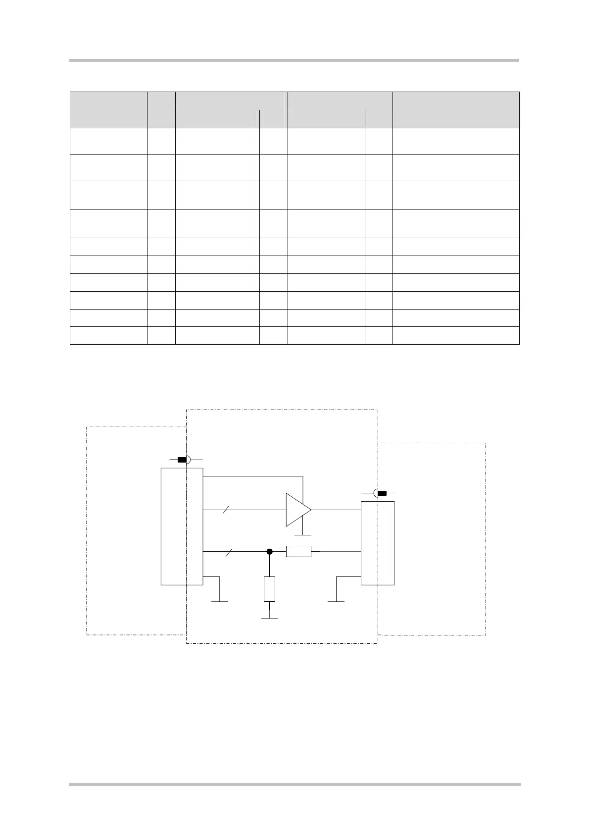
DSB75
X703
25 pole
D-Sub
10 pole
GSM
audio tester
(e.g. R&S UPL16)
with
GSM 11.10
DAI interface
DAI adapter
5V0
1
e.g.
74HCT4050
2x
2
2
2x
2x
Figure 20: Example for connecting measurement equipment