DSB75 Development Support Board Rev. B1 Hardware Description
Confidential / Released
DSB75_hd_v12 Page 44 of 96 2008-08-26
X201 X205
X400
X401
X110
X120
S112
S110
X121
S111
S457
S452
S456
S455
S453S454
S450
S460
S451
S461S462
S464S465 S463
S466
S469S459
S467
S458
S468
1
1
1
1
1 4 2 3
15
69
15
69
13
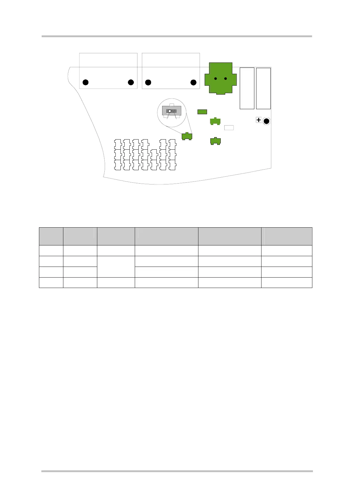
Figure 22: Location of the USB interface, switches and jumper
Table 17: Pin assignment of USB device interface X110
X110
pin
Name I/O Description X100 signal name Config.
switches
1 VBUS I (Supply) USB bus voltage VUSB_IN S110:3
2 D- Data line minus USB_DN S111:3
3 D+
Diff. I/O
Data line plus USB_DP S112:3
4 GND Supply GND GND