DSB75 Development Support Board Rev. B1 Hardware Description
Confidential / Released
DSB75_hd_v12 Page 47 of 96 2008-08-26
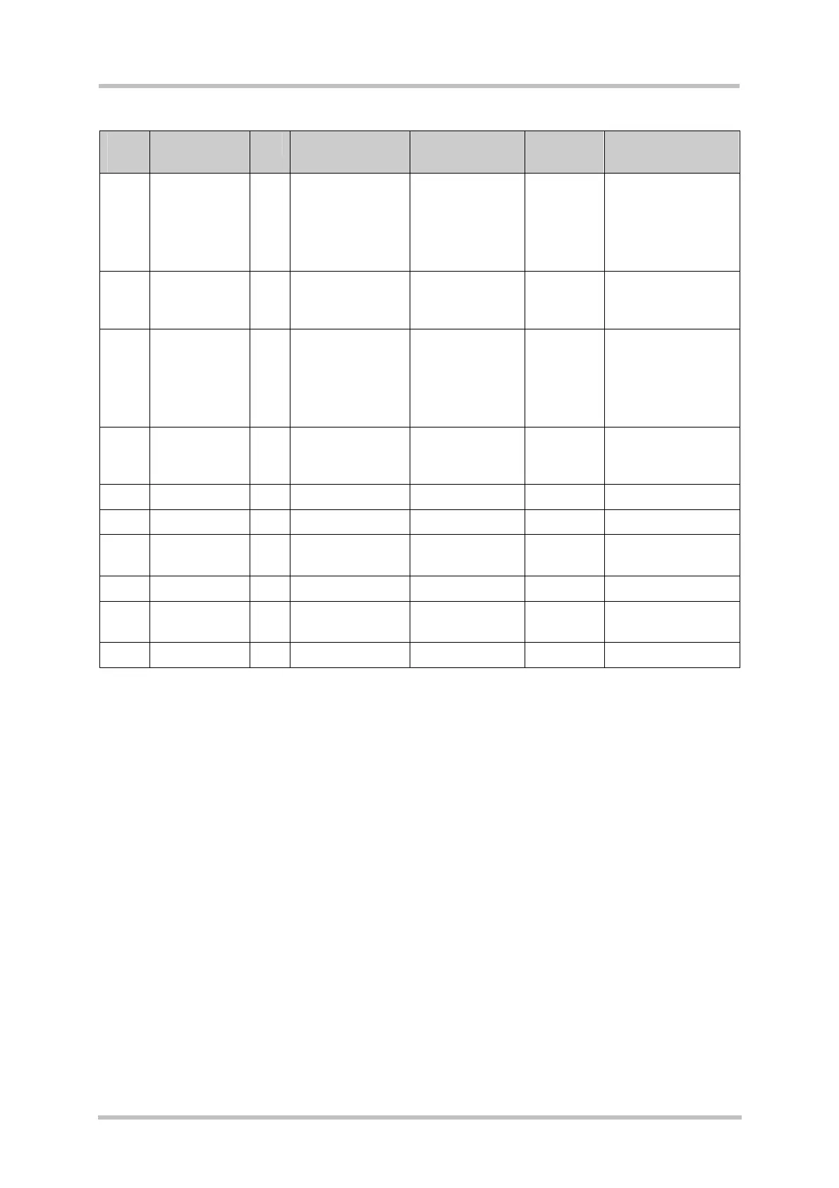
Table 18: Pin assignment of the I²C interface X511
X511
pin
Name I/O Description X100 signal
name
Config.
switches
Remark
1 I2C_CLK_5V O Clock,
(5V logic)
I2CCLK S500:3 EEPROM
accessible
External pull-up
resistor 3k3
recommended
2 I2C_CLK_3V O Clock,
(3V logic)
I2CCLK S500:1 External pull-up
resistor 750R
required
3 I2C_DAT_5V I/O Data,
(5V logic)
I2CDAT S501:3 EEPROM
accessible
External pull-up
resistor 3k3
recommended
4 I2C_DAT_3V I/O Data,
(3V logic)
ISCDAT S501:1 External pull-up
resistor 750R
required
5 n.c.
6 n.c.
7 5V0 O 5V0 supply
voltage
ON when DSB75
is supplied
8 GND Ground
9 VDD O 2.9V supply
voltage
ON when GSM
module is active
10 GND Ground