DSB75 Development Support Board Rev. B1 Hardware Description
Confidential / Released
DSB75_hd_v12 Page 34 of 96 2008-08-26
3.5.2 Serial Interface 2 (COM2)
The 2
nd
serial interface COM2 (X202) of the DSB75 is intended for the communication
between the GSM module and the host application. This RS-232C interface includes only the
data lines RXD/TXD for transmitting GPRS data and AT commands, and the two control
lines RTS/CTS.
A level converter D201 adapts and inverts the V.24 signals (2.9V level) from the GSM
module to the RS-232C level.
The output lines are switched off (high impedance) if the GSM module is in POWER DOWN
mode. Therefore the PWR_IND signal is used to enable and shut down converters.
There are two alternative approaches to configure the ASC1 lines:
• as SD card interface (see section
3.10.2)
• as SPI interface (see section
3.10.3)
For using ASC1 lines at the test pins X101/X102 without a RS-232 level shifter, the switches
S300, S302, S304 and S306 have to be set to position 1.
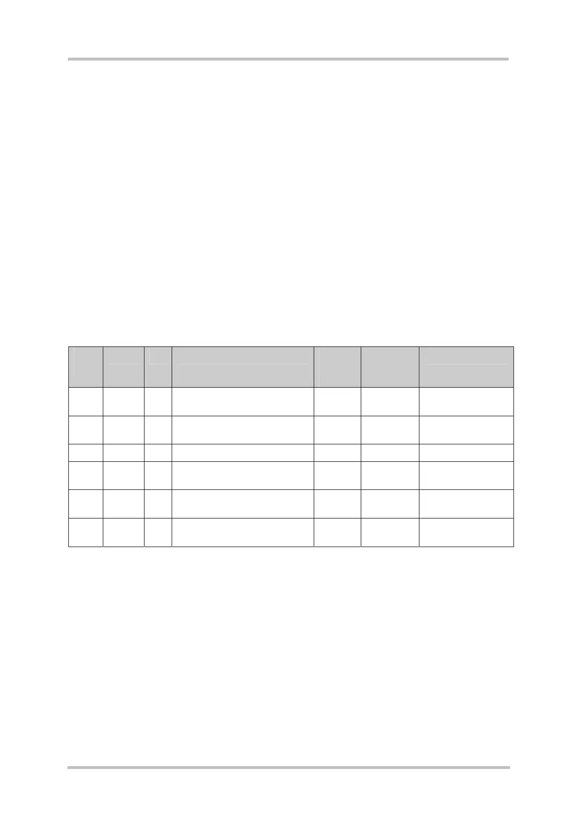
Table 12: Pin assignment of 2
nd
serial interface COM2 (X202)
X202
pin
Name I/O Description X100
signal
name
Config.
switches
Remark
2 RXD O Receive Data RXD1 S302:3
S303:1
3 TXD I Transmit Data TXD1 S300:3
S301:1
5 GND - Ground GND
7 RTS I Request To Send RTS1 S304:3
S305:1
8 CTS O Clear To Send CTS1 S306:3
S307:1
1, 4,
6, 9
nc
nc= not connected