DSB75 Development Support Board Rev. B1 Hardware Description
Confidential / Released
DSB75_hd_v12 Page 54 of 96 2008-08-26
S110
X510
X511
X551
X552
S307S305S303
S301
S300S302
S304S3 06
S713
S712
S717S716
X101
X102
S201
S2 00 X554
X703
X561
X560
X562
S504
S503
S502
S501
S500
S457
S452
S456
S455
S453
S454
S450
S460
S451
S461S462
S464S465
S463
S466
S469
S459
S467
S458
S468
1
10
39
40
1
2
1
1
39
40
1
2
1
1
1
2
2
9
10
9
10
2
9
1
3
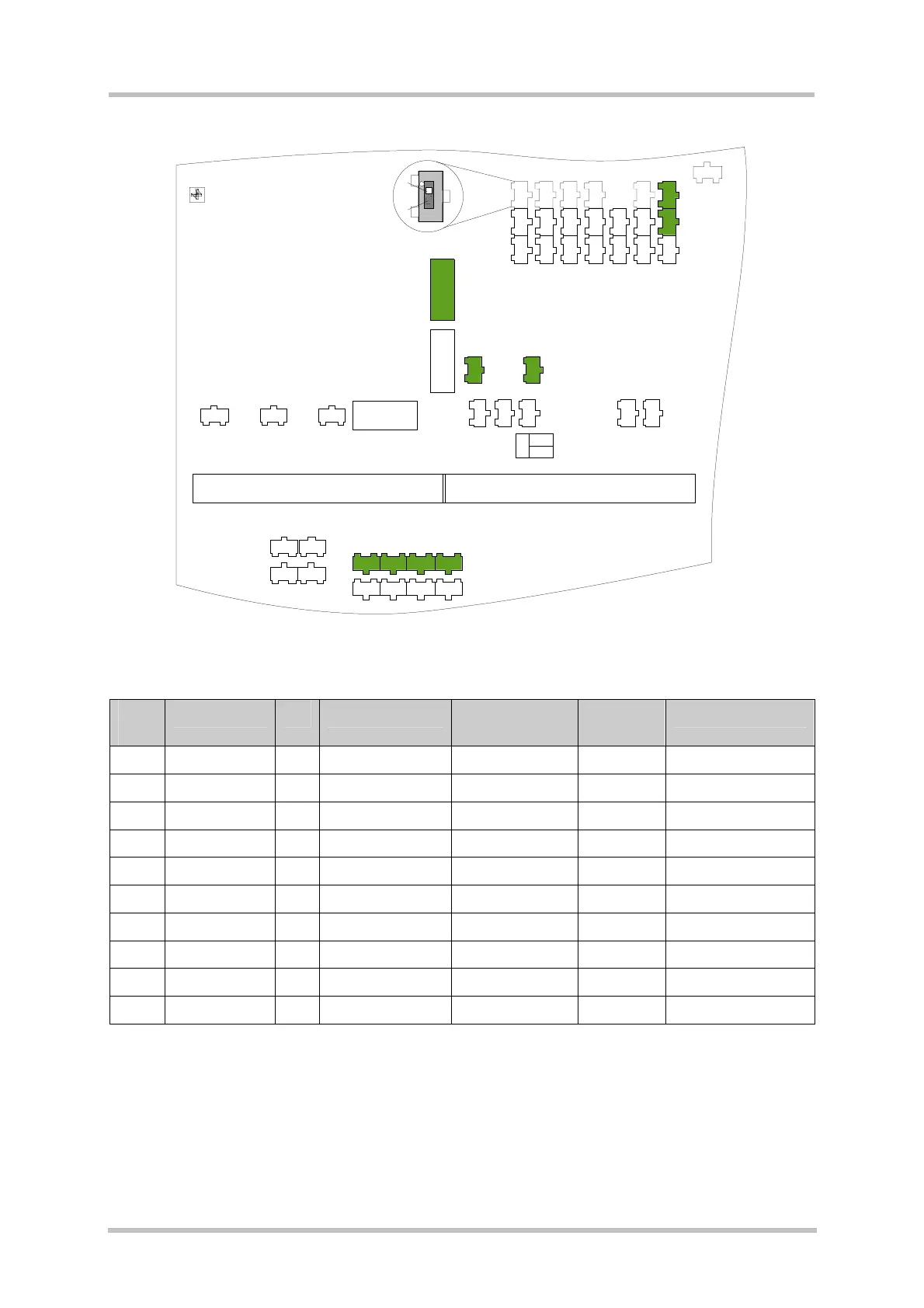
Figure 28: SPI interfaces location and related switches
Table 23: Pin assignment of the SPI interfaces X510
X510
pin
Name I/O Description X100 signal
name
Config.
switches
Remark
1 CS2 O Chip select 2 TXD1 S300:1
2 CS1 O Chip select 1 SPICS S456:1
3 DI2 I Data in 2 RXD1 S302:1
4 DI1 I Data in 1 SPIDI S457:1
5 SCLK2 O Clock 2 RTS1 S304:1
6 SCLK1 O Clock 1 I2CCLK S500:1
7 DO2 O Data out 2 CTS1 S306:1
8 DO1 O Data out 1 I2CDAT S501:1
9 VDD O 2.9V supply out
10 GND