DSB75 Development Support Board Rev. B1 Hardware Description
Confidential / Released
DSB75_hd_v12 Page 83 of 96 2008-08-26
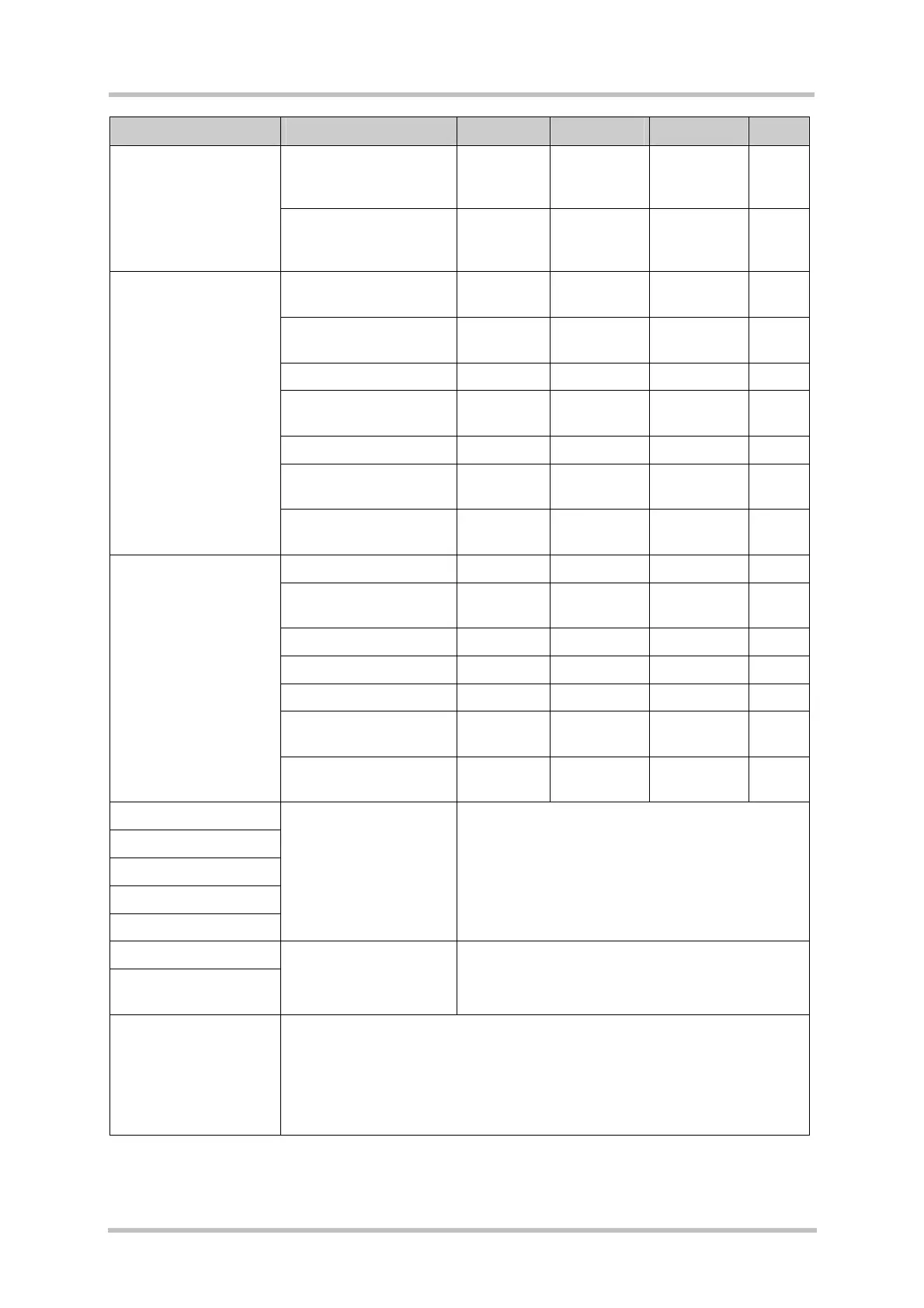
Parameters Condition Min. Typical Max. Unit
Differential output
voltage at full scale sine
1kHz
1.6 Vpp
Audio interface 1
(balanced input)
Handset Mode
(AT^SNFS=1)
Differential input
voltage for 0dBm0
(after settling)
30 mV
Maximum differential
output voltage, no load
6.0 Vpp
Differential output
resistance
15
Differential output load 0
Differential input
voltage
1.6 V
Input impedance 4.0 k
Microphone supply
voltage
5.0 V
Audio interface 1
(balanced input)
General Information
Microphone supply DC
resistance
4.6 k
Output voltage 3.4 Vpp
Differential output
resistance
15
Differential output load 16
Input voltage 1.6 V
Input impedance 2.0 k
Microphone supply
voltage
2.5 V
Audio interface 2
(single ended input)
General Information
Microphone supply DC
resistance
2.2 k
SPI interface
Digital audio interface
SIM interface
USB interface
SD card interface
The interface lines are
connected directly to
the GSM module
See module specification
[1] for details.
Ignition (Key)
Emergency Restart
(Key)
Ignition via DTR line
@COM1
V
I
= ±3V…±9V: V
I
>±9V:
signal
~~~
|________|
~~~~~~~~~~~~~~~
signal
~~~
|________|
~~~~~~~~~~~~~~~
| 1s | 0.5s | | 0.5s | 0.5s |
Rise time 1ms.
Low high transition of this signal switches the module on.