Signal Description
80 Datasheet, Volume 1
6.3 Reset and Miscellaneous Signals
6.4 PCI Express* Based Interface Signals
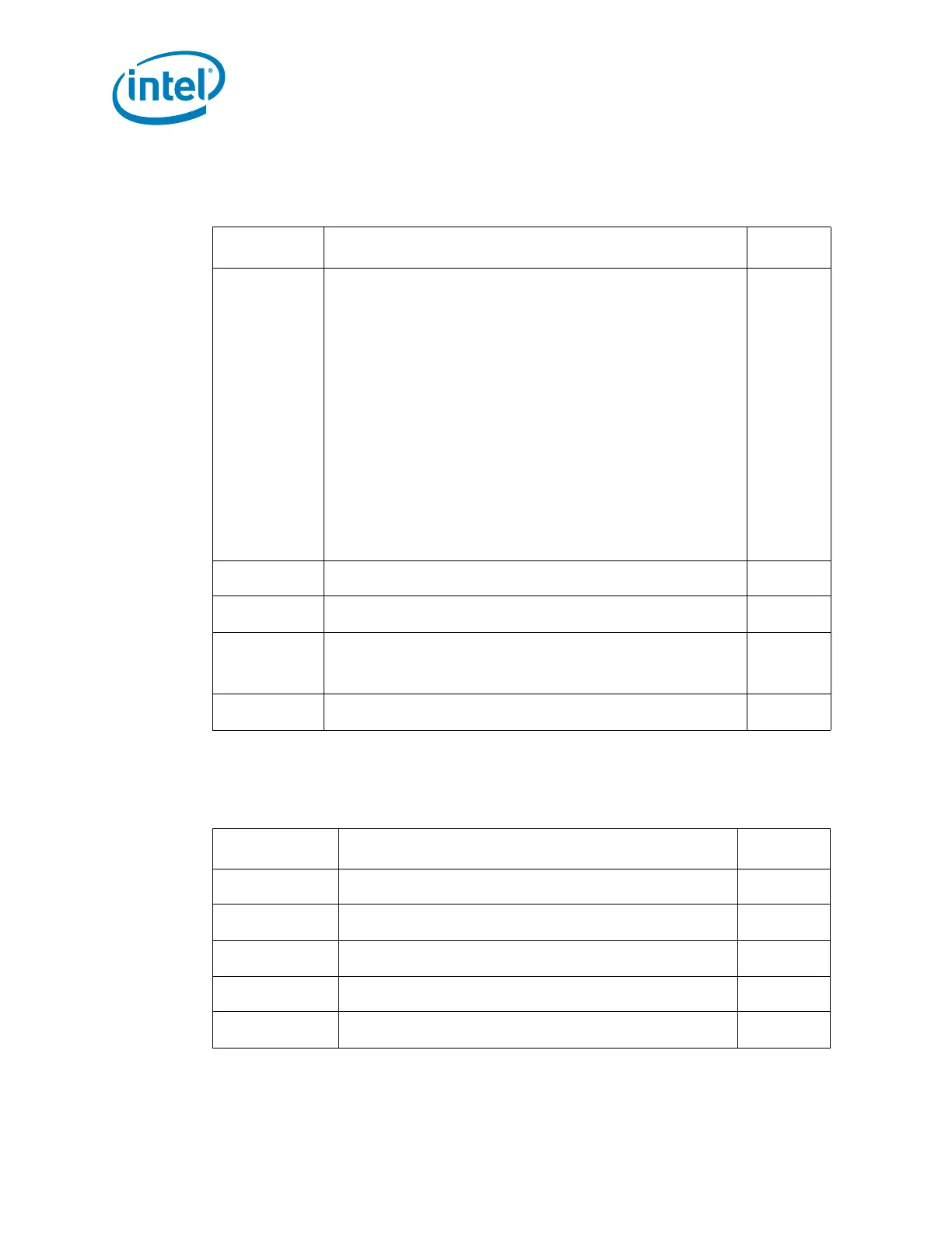
Table 6-5. Reset and Miscellaneous Signals
Signal Name Description
Direction/
Buffer Type
CFG[17:0]
Configuration Signals: The CFG signals have a default value of '1' if not
terminated on the board.
•CFG[1:0]: Reserved configuration lane. A test point may be placed on
the board for this lane.
• CFG[2]: PCI Express* Static x16 Lane Numbering Reversal.
— 1 = Normal operation
— 0 = Lane numbers reversed
• CFG[3]: Reserved
• CFG[4]: eDP enable
—1 = Disabled
—0 = Enabled
• CFG[6:5]: PCI Express Bifurcation:
— 00 = 1 x8, 2 x4 PCI Express
— 01 = reserved
— 10 = 2 x8 PCI Express
— 11 = 1 x16 PCI Express
• CFG[17:7]: Reserved configuration lanes. A test point may be placed
on the board for these lands.
I
CMOS
PM_SYNC
Power Management Sync: A sideband signal to communicate power
management status from the platform to the processor.
I
CMOS
RESET#
Platform Reset pin driven by the PCH I
CMOS
RSVD
RSVD_TP
RSVD_NCTF
RESERVED: All signals that are RSVD and RSVD_NCTF must be left
unconnected on the board. However, Intel recommends that all RSVD_TP
signals have using test points.
No Connect
Tes t Po in t
Non-Critical
to Function
SM_DRAMRST#
DDR3 DRAM Reset: Reset signal from processor to DRAM devices. One
common to all channels.
O
CMOS
Table 6-6. PCI Express* Graphics Interface Signals
Signal Name Description
Direction/
Buffer Type
PEG_ICOMPI
PCI Express Input Current Compensation I
A
PEG_ICOMPO
PCI Express Current Compensation I
A
PEG_RCOMPO
PCI Express Resistance Compensation I
A
PEG_RX[15:0]
PEG_RX#[15:0]
PCI Express Receive Differential Pair I
PCI Express
PEG_TX[15:0]
PEG_TX#[15:0]
PCI Express Transmit Differential Pair O
PCI Express

 Loading...


