Datasheet, Volume 1 95
Electrical Specifications
Notes:
1. Refer to Chapter 6 for signal description details.
2. SA and SB refer to DDR3 Channel A and DDR3 Channel B.
3. These signals only apply to BGA packages.
4. The maximum rise/fall time of UNCOREPWRGOOD is 20 ns.
All Control Sideband Asynchronous signals are required to be asserted/de-asserted for
at least 10 BCLKs with a maximum Trise/Tfall of 6 ns for the processor to recognize
the proper signal state. See Section 7.10 for the DC specifications.
7.7 Test Access Port (TAP) Connection
Due to the voltage levels supported by other components in the Test Access Port (TAP)
logic, Intel recommends the processor be first in the TAP chain, followed by any other
components within the system. A translation buffer should be used to connect to the
rest of the chain unless one of the other components is capable of accepting an input of
the appropriate voltage. Two copies of each signal may be required with each driving a
different voltage level.
The processor supports Boundary Scan (JTAG) IEEE 1149.1-2001 and IEEE 1149.6-
2003 standards. Note that some small portion of the I/O pins may support only one of
these standards.
7.8 Storage Condition Specifications
Environmental storage condition limits define the temperature and relative humidity
that the device is exposed to while being stored in a moisture barrier bag. The specified
storage conditions are for component level prior to board attach.
Table 7-5 specifies absolute maximum and minimum storage temperature limits that
represent the maximum or minimum device condition beyond which damage, latent or
otherwise, may occur. The table also specifies sustained storage temperature, relative
humidity, and time-duration limits. These limits specify the maximum or minimum
device storage conditions for a sustained period of time. Failure to adhere to the
following specifications can affect long term reliability of the processor.
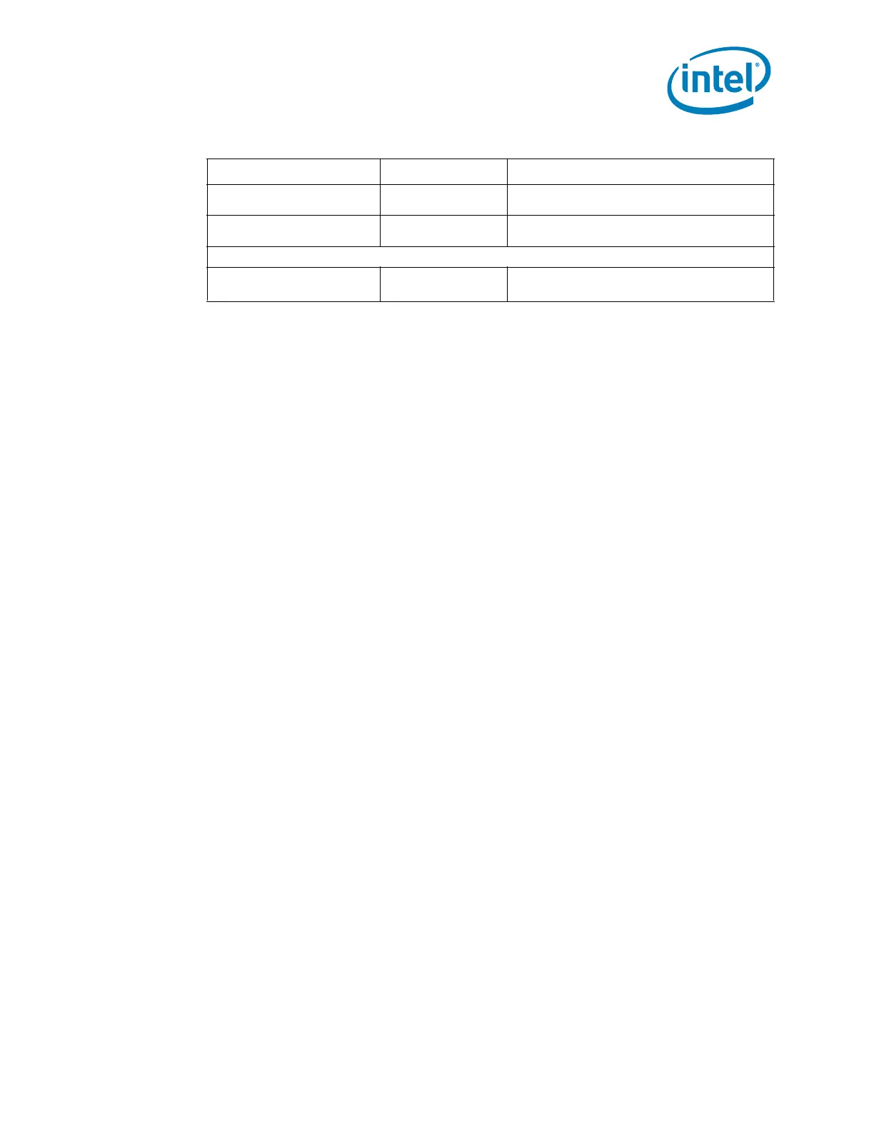
Single Ended
Asynchronous CMOS
Input
FDI_INT
Differential FDI Output
FDI0_TX[3:0], FDI0_TX#[3:0], FDI1_TX[3:0],
FDI1_TX#[3:0]
Future Compatibility
PROC_SELECT#, VCCSA_VID[0], VCCIO_SEL,
SA_DIMM_VREFDQ, SB_DIMM_VREFDQ
Table 7-3. Signal Groups
1
(Sheet 3 of 3)
Signal Group Type Signals

 Loading...


