Datasheet, Volume 1 93
Electrical Specifications
7.6 Signal Groups
Signals are grouped by buffer type and similar characteristics as listed in Table 7-3. The
buffer type indicates which signaling technology and specifications apply to the signals.
All the differential signals, and selected DDR3 and Control Sideband signals, have On-
Die Termination (ODT) resistors. There are some signals that do not have ODT and
need to be terminated on the board.
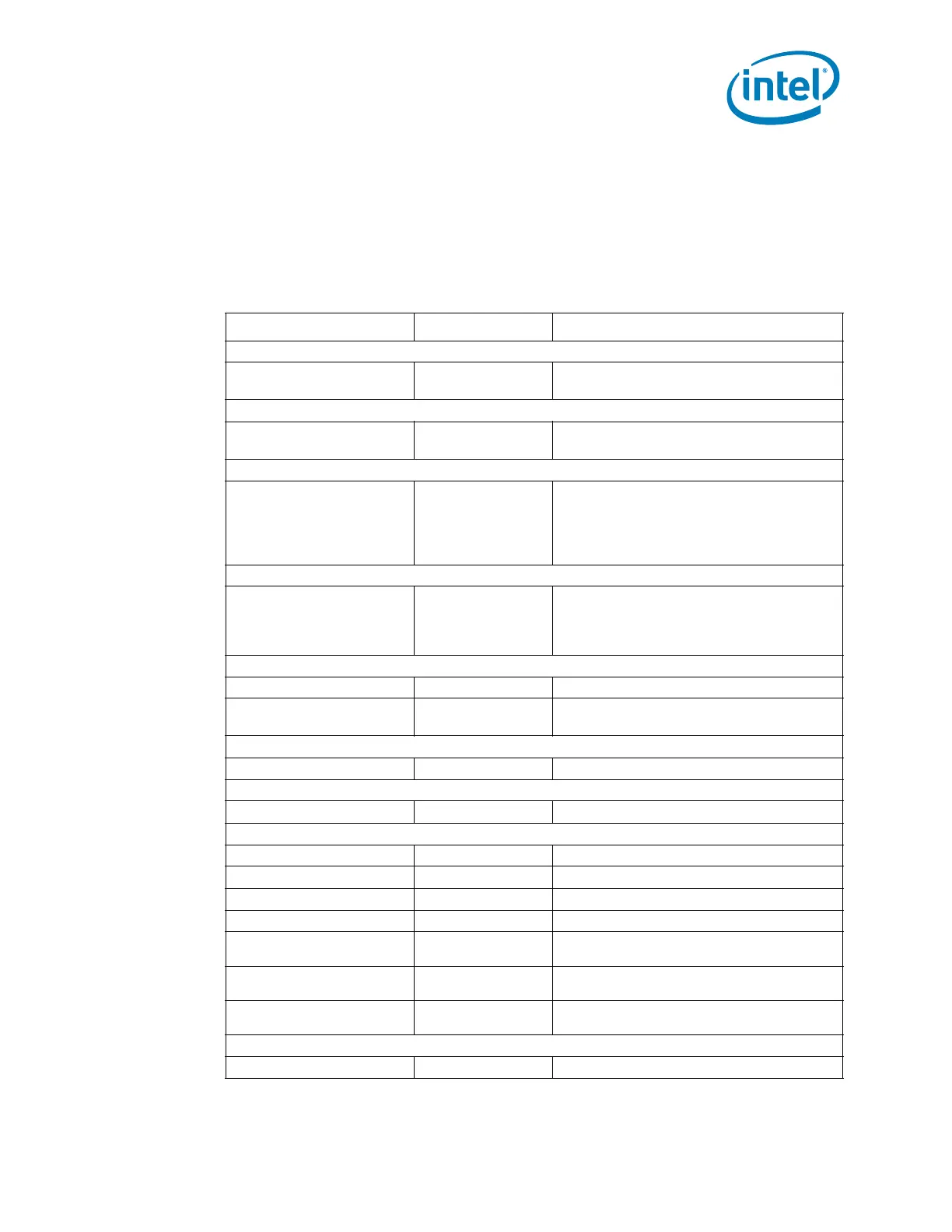
Table 7-3. Signal Groups
1
(Sheet 1 of 3)
Signal Group Type Signals
System Reference Clock
Differential CMOS Input
BCLK, BCLK#
DPLL_REF_CLK, DPLL_REF_CLK#
DDR3 Reference Clocks
2
Differential DDR3 Output
SA_CK[1:0], SA_CK#[1:0]
SB_CK[1:0], SB_CK#[1:0]
DDR3 Command Signals
2
Single Ended DDR3 Output
SA_BS[2:0], SB_BS[2:0]
SA_WE#, SB_WE#
SA_RAS#, SB_RAS#
SA_CAS#, SB_CAS#
SA_MA[15:0], SB_MA[15:0]
DDR3 Control Signals
2
Single Ended DDR3 Output
SA_CKE[1:0], SB_CKE[1:0]
SA_CS#[1:0], SB_CS#[1:0]
SA_ODT[1:0], SB_ODT[1:0]
SM_DRAMRST#
DDR3 Data Signals
2
Single ended DDR3 Bi-directional SA_DQ[63:0], SB_DQ[63:0]
Differential DDR3 Bi-directional
SA_DQS[7:0], SA_DQS#[7:0]
SB_DQS[7:0], SB_DQS#[7:0]
DDR3 Compensation
Analog Bi-directional SM_RCOMP[2:0]
DDR3 Reference
Analog Input SM_VREF
TAP (ITP/XDP)
Output BCLK_ITP, BCLK_ITP#
Single Ended CMOS Input TCK, TDI, TMS, TRST#
Single Ended Open-Drain Output TDO
Single Ended Output DBR#
Single Ended
Asynchronous CMOS
Bi-Directional
BPM#[7:0]
Single Ended
Asynchronous CMOS
Input
PREQ#
Single Ended
Asynchronous CMOS
Output
PRDY#
Control Sideband
Single Ended CMOS Input CFG[17:0]

 Loading...


