Datasheet, Volume 1 85
Signal Description
6.14 Ground and NCTF
6.15 Future Compatibility
6.16 Processor Internal Pull Up/Pull Down
§ §
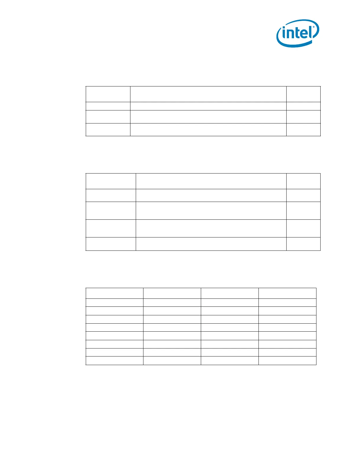
Table 6-16. Ground and NCTF
Signal Name Description
Direction/
Buffer Type
VSS Processor ground node GND
VSS_NCTF
(BGA Only)
Non-Critical to Function: These pins are for package mechanical
reliability.
DC_TEST_xx#
Daisy Chain- These pins are for solder joint reliability and non-critical to
function. For BGA only.
Table 6-17. Future Compatibility
Signal Name Description
Direction/
Buffer Type
PROC_SELECT#
This pin is for compatibility with future platforms. A pull-up resistor
to V
CPLL
is required if connected to the DF_TVS strap on the PCH.
SA_DIMM_VREFDQ
SB_DIMM_VREFDQ
Memory Channel A/B DIMM DQ Voltage Reference: These
signals are not used by the processors and are for future compatibility
only. No connection is required.
VCCIO_SEL
Voltage selection for VCCIO: This pin must be pulled high on the
motherboard, when using dual rail voltage regulator, which will be
used for future compatibility.
VCCSA_VID[0]
Voltage selection for VCCSA: This pin must have a pull down
resistor to ground.
Table 6-18. Processor Internal Pull Up/Pull Down
Signal Name Pull Up/Pull Down Rail Value
BPM[7:0] Pull Up VCCIO 65–165
PRDY# Pull Up VCCIO 65–165
PREQ# Pull Up VCCIO 65–165
TCK Pull Down VSS 5–15 k
TDI Pull Up VCCIO 5–15 k
TMS Pull Up VCCIO 5–15 k
TRST# Pull Up VCCIO 5–15 k
CFG[17:0] Pull Up VCCIO 5–15 k

 Loading...


