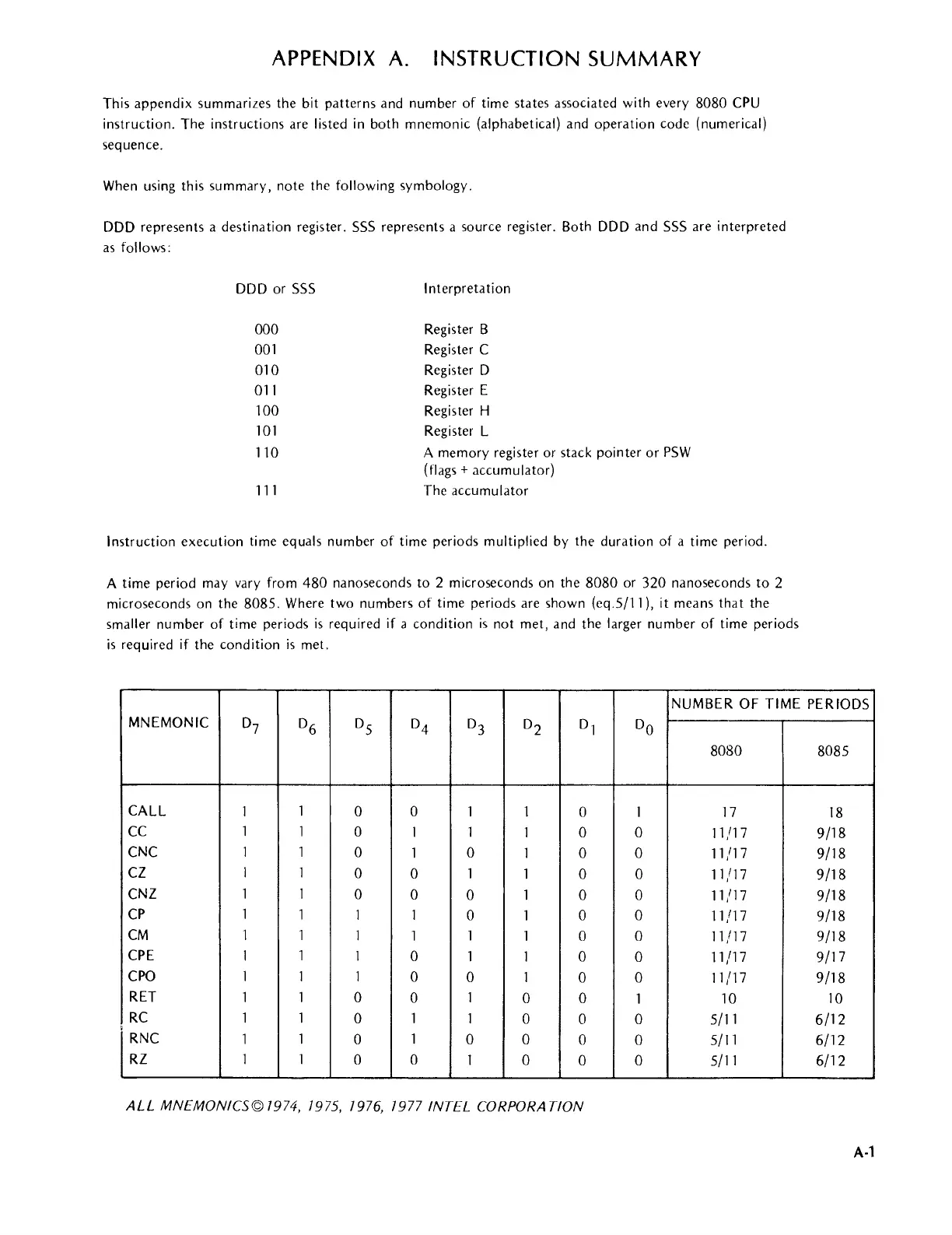
APPENDIX
A.
INSTRUCTION
SUMMARY
This appendix summarizes the bit patterns and number
of
time states associated with every 8080
CPU
instruction. The instructions are listed
in
both mnemonic (alphabetical) and operation code (numerical)
sequence.
When using this summary, note the
following symbology.
DDD
represents a destination register.
SSS
represents a source register. Both
DDD
and
SSS
are interpreted
as
follows:
DDD
or
SSS
000
001
010
011
100
101
110
111
Interpretation
Register B
Register
C
Register D
Register E
Register H
Register L
A memory register or stack pointer or
PSW
(flags + accumulator)
The accumulator
Instruction execution time equals number
of
time periods multiplied by the duration of a time period.
A time period may vary from
480
nanoseconds to 2 microseconds on the
8080
or 320 nanoseconds to 2
microseconds on the
8085. Where two numbers
of
time periods are shown (eq.5/11), it means that the
smaller number
of
time periods
is
required if a condition
is
not met, and the larger number
of
time periods
is
required if the condition
is
met.
NUMBER
OF TIME PERIODS
MNEMONIC
D7
D6
D5
D4
D3
D2
Dl
DO
8080
8085
CALL
1
1
0 0
1 1
0 I 17
18
CC
1 1
0
1 1
1
0 0
11/17
9/18
CNC 1 1
0
1
0
1 0 0
11
/17 9/18
CZ
I 1
0
0
1
1
0 0
11/17
9/18
CNZ 1 1
0
0
0 1 0 0
11/17 9/18
CP
1
1
1 1
0
1
0 0
11/17
9/18
CM
1 1
1
1 1
1
0 0
11/17
9/18
CPE
1
1
1
0
1 1 0
0
11/17
9/17
CPO
1 1 1
0
0
1
0 0
11/17
9/18
RET
1 1 0
0
1
0 0
1
10
10
RC
1 1
0 1 1
0
0 0
5/11
6/12
•
RNC
1 1
0
1
0 0
0
0
5/11
6/12
RZ
1 1
0 0
1 0
0 0
5/11
6/12
ALL
MNEMONICS© 1974, 1975, 1976, 1977 INTEL
CORPORA
nON
A-l