Datasheet, Volume 1 61
Signal Description
6 Signal Description
This chapter describes the processor signals. They are arranged in functional groups
according to their associated interface or category. The following notations are used to
describe the signal type.
The signal description also includes the type of buffer used for the particular signal (see
Ta b le 6- 1).
Notes:
1. Qualifier for a buffer type.
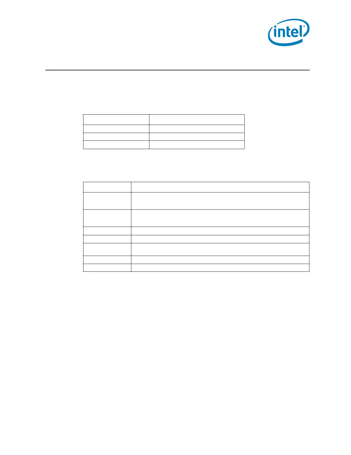
Notations Signal Type
IInput Pin
OOutput Pin
I/O Bi-directional Input/Output Pin
Table 6-1. Signal Description Buffer Types
Signal Description
PCI Express*
PCI Express interface signals. These signals are compatible with PCI Express* 2.0
Signalling Environment AC Specifications and are AC coupled. The buffers are not
3.3-V tolerant. Refer to the PCIe specification.
DMI
Direct Media Interface signals. These signals are based on PCI Express* 2.0 Signaling
Environment AC Specifications (5 GT/s), but are DC coupled. The buffers are not
3.3-V tolerant.
CMOS CMOS buffers. 1.1-V tolerant
DDR3 DDR3 buffers: 1.5-V tolerant
A
Analog reference or output. May be used as a threshold voltage or for buffer
compensation
Ref Voltage reference signal
Asynchronous
1
Signal has no timing relationship with any reference clock.