Electrical Specifications
76 Datasheet, Volume 1
7.5 System Agent (SA) VCC VID
The VCC
SA
is configured by the processor output pin VCCSA_VID.
VCCSA_VID output default logic state is low for the processors; logic high is reserved
for future compatibility.
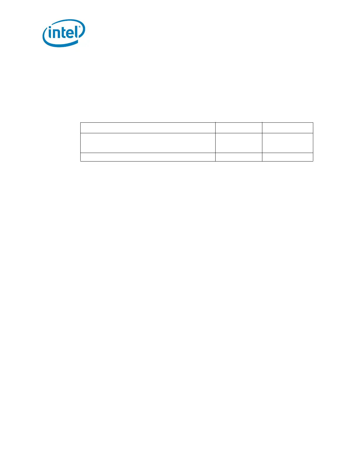
Tab l e 7 -2 specifies the different VCCSA_VID configurations.
Notes:
1. Some of V
CCSA
configurations are reserved for future Intel processor families.
7.6 Reserved or Unused Signals
The following are the general types of reserved (RSVD) signals and connection
guidelines:
• RSVD – These signals should not be connected.
• RSVD_NCTF – These signals are non-critical to function and may be left un-
connected
Arbitrary connection of these signals to V
CC
, V
CCIO
, V
DDQ
, V
CCPLL
, V
CCSA,
V
CCAXG,
V
SS
, or
to any other signal (including each other) may result in component malfunction or
incompatibility with future processors. See Chapter 8 for a land listing of the processor
and the location of all reserved signals.
For reliable operation, always connect unused inputs or bi-directional signals to an
appropriate signal level. Unused active high inputs should be connected through a
resistor to ground (V
SS
). Unused outputs maybe left unconnected; however, this may
interfere with some Test Access Port (TAP) functions, complicate debug probing, and
prevent boundary scan testing. A resistor must be used when tying bi-directional
signals to power or ground. When tying any signal to power or ground, a resistor will
also allow for system testability. For details see Table 7- 9 .
Table 7-2. VCCSA_VID configuration
Processor Family VCCSA_VID Selected VCCSA
2nd Generation Intel
®
Core™ processor family desktop,
Intel
®
Pentium
®
processor family desktop,
Intel
®
Celeron
®
processor family desktop
0 0.925 V
Future Intel processors 1 Note 1
 Loading...