Datasheet, Volume 1 77
Electrical Specifications
7.7 Signal Groups
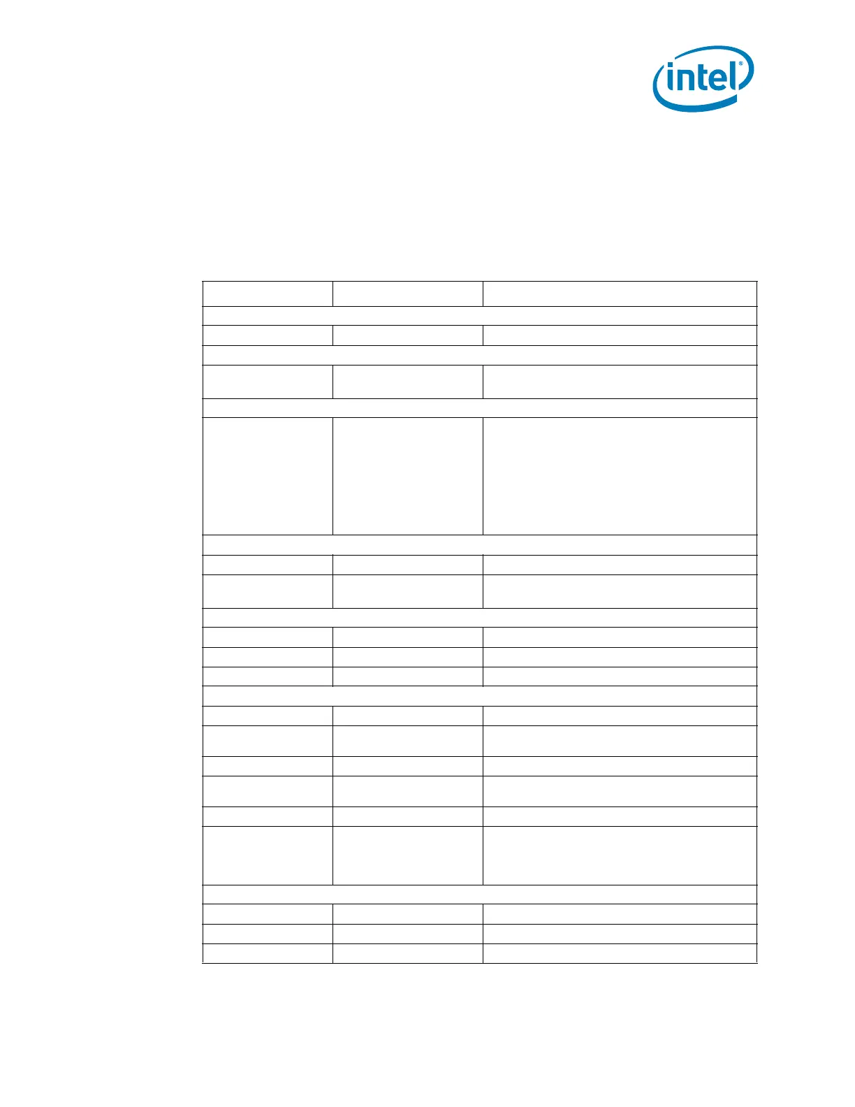
Signals are grouped by buffer type and similar characteristics as listed in Table 7- 3 . The
buffer type indicates which signaling technology and specifications apply to the signals.
All the differential signals, and selected DDR3 and Control Sideband signals have On-
Die Termination (ODT) resistors. There are some signals that do not have ODT and
need to be terminated on the board.
Table 7-3. Signal Groups (Sheet 1 of 2)
1
Signal Group Type Signals
System Reference Clock
Differential CMOS Input BCLK[0], BCLK#[0]
DDR3 Reference Clocks
2
Differential DDR3 Output
SA_CK[3:0], SA_CK#[3:0]
SB_CK[3:0], SB_CK#[3:0]
DDR3 Command Signals
2
Single Ended DDR3 Output
SA_RAS#, SB_RAS#, SA_CAS#, SB_CAS#
SA_WE#, SB_WE#
SA_MA[15:0], SB_MA[15:0]
SA_BS[2:0], SB_BS[2:0]
SM_DRAMRST#
SA_CS#[3:0], SB_CS#[3:0]
SA_ODT[3:0], SB_ODT[3:0]
SA_CKE[3:0], SB_CKE[3:0]
DDR3 Data Signals
2
Single ended DDR3 Bi-directional SA_DQ[63:0], SB_DQ[63:0]
Differential DDR3 Bi-directional
SA_DQS[8:0], SA_DQS#[8:0]
SB_DQS[8:0], SB_DQS#[8:0]
TAP (ITP/XDP)
Single Ended CMOS Input TCK, TDI, TMS, TRST#
Single Ended CMOS Output TDO
Single Ended Asynchronous CMOS Output TAPPWRGOOD
Control Sideband
Single Ended CMOS Input CFG[17:0]
Single Ended
Asynchronous CMOS/Open
Drain Bi-directional
PROCHOT#
Single Ended Asynchronous CMOS Output THERMTRIP#, CATERR#
Single Ended Asynchronous CMOS Input
SM_DRAMPWROK, UNCOREPWRGOOD
3
, PM_SYNC,
RESET#
Single Ended Asynchronous Bi-directional PECI
Single Ended
CMOS Input
Open Drain Output
Bi-directional CMOS Input
/Open Drain Output
VIDALERT#
VIDSCLK
VIDSOUT
Power/Ground/Other
Power VCC, VCC_NCTF, VCCIO, VCCPLL, VDDQ, VCCAXG
Ground VSS
No Connect and test point RSVD, RSVD_NCTF, RSVD_TP, FC_x