Electrical Specifications
84 Datasheet, Volume 1
Notes:
1. Unless otherwise noted, all specifications in this table apply to all processor frequencies.
2. V
IL
is defined as the maximum voltage level at a receiving agent that will be interpreted as a logical low
value.
3. V
IH
is defined as the minimum voltage level at a receiving agent that will be interpreted as a logical high
value.
4. V
IH
and V
OH
may experience excursions above V
DDQ
. However, input signal drivers must comply with the
signal quality specifications.
5. This is the pull up/down driver resistance.
6. R
TERM
is the termination on the DIMM and in not controlled by the processor.
7. The minimum and maximum values for these signals are programmable by BIOS to one of the two sets.
8. DDR3 values are pre-silicon estimations and subject to change.
9. SM_DRAMPWROK must have a maximum of 15 ns rise or fall time over V
DDQ
* 0.55 ±200 mV and edge
must be monotonic.
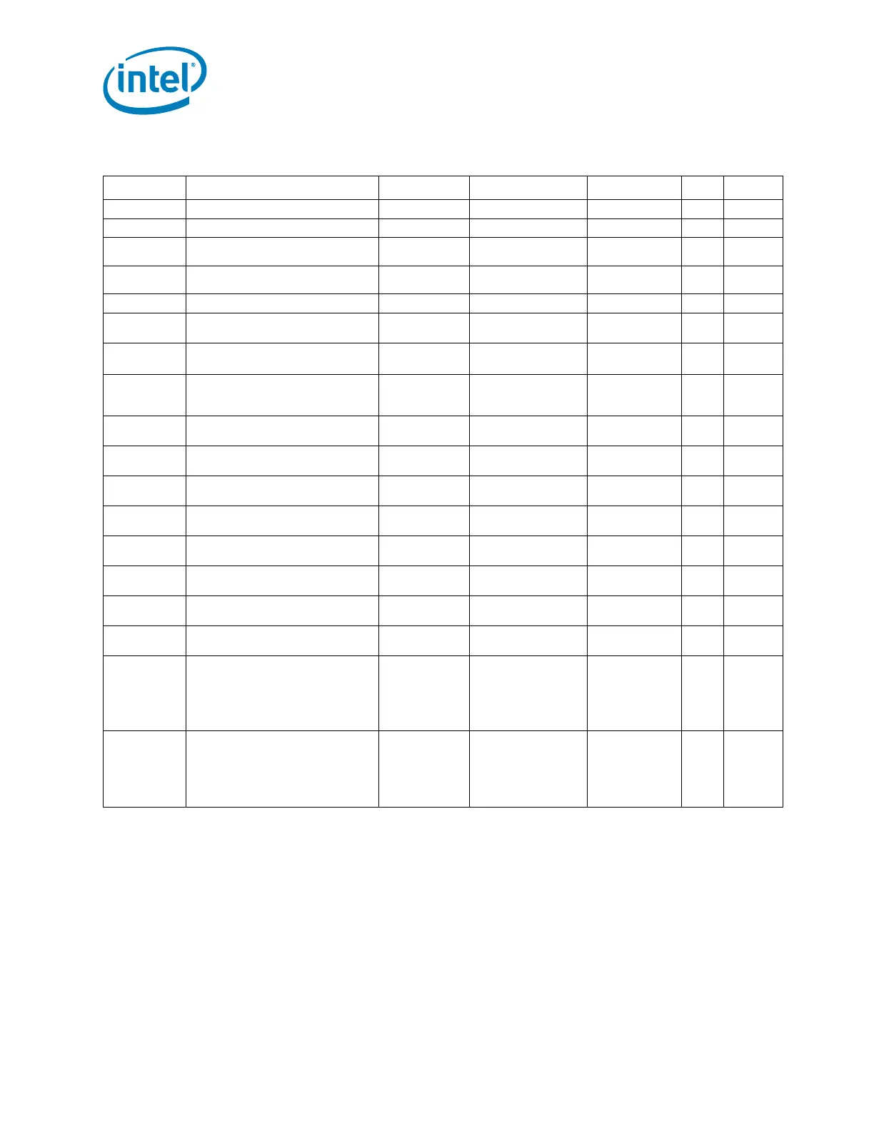
Table 7-8. DDR3 Signal Group DC Specifications
Symbol Parameter Min Typ Max Units Notes
1,9
V
IL
Input Low Voltage — — SM_VREF – 0.1 V 2,4
V
IH
Input High Voltage SM_VREF + 0.1 — — V 3
V
OL
Output Low Voltage
—
(V
DDQ
/ 2)* (R
ON
/(R
ON
+R
TERM
))
—6
V
OH
Output High Voltage
—
V
DDQ
– ((V
DDQ
/ 2)*
(R
ON
/(R
ON
+R
TERM
))
—V4,6
R
ON_UP(DQ)
DDR3 data buffer pull-up resistance 24.31 28.6 32.9 Ω 5
R
ON_DN(DQ)
DDR3 data buffer pull-down
resistance
22.88 28.6 34.32 Ω 5
R
ODT(DQ)
DDR3 on-die termination equivalent
resistance for data signals
83
41.5
100
50
117
65
Ω 7
V
ODT(DC)
DDR3 on-die termination DC
working point (driver set to receive
mode)
0.43*V
DDQ
0.5*V
DDQ
0.56*V
CC
V7
R
ON_UP(CK)
DDR3 clock buffer pull-up
resistance
20.8 26 28.6 Ω 5
R
ON_DN(CK)
DDR3 clock buffer pull-down
resistance
20.8 26 31.2 Ω 5
R
ON_UP(CMD)
DDR3 command buffer pull-up
resistance
16 20 23 Ω 5
R
ON_DN(CMD)
DDR3 command buffer pull-down
resistance
16 20 24 Ω 5
R
ON_UP(CTL)
DDR3 control buffer pull-up
resistance
16 20 23 Ω 5
R
ON_DN(CTL)
DDR3 control buffer pull-down
resistance
16 20 24 Ω 5
V
IL_SM_DRAMP
WROK
Input Low Voltage for
SM_DRAMPWROK
——V
DDQ
*.55 – 0.1 V 9
V
IH_SM_DRAMP
WROK
Input High Voltage for
SM_DRAMPWROK
V
DDQ
*.55 +0.1 — — V 9
I
LI
Input Leakage Current (DQ, CK)
0V
0.2*V
DDQ
0.8*V
DDQ
V
DDQ
——
± 0.75
± 0.55
± 0.9
± 1.4
mA
I
LI
Input Leakage Current (CMD, CTL)
0V
0.2*V
DDQ
0.8*V
DDQ
V
DDQ
——
± 0.85
± 0.65
± 1.1
± 1.65
mA