Electrical Specifications
30 Datasheet
3.7 FSB Signal Groups
The FSB signals have been combined into groups by buffer type in the following
sections. In this document, the term “AGTL+ Input” refers to the AGTL+ input group as
well as the AGTL+ I/O group when receiving. Similarly, “AGTL+ Output” refers to the
AGTL+ output group as well as the AGTL+ I/O group when driving.
With the implementation of a source-synchronous data bus, two sets of timing
parameters are specified. One set is for common clock signals, which are dependent
upon the rising edge of BCLK0 (ADS#, HIT#, HITM#, etc.), and the second set is for
the source-synchronous signals which are relative to their respective strobe lines (data
and address) as well as the rising edge of BCLK0. Asychronous signals are still present
(A20M#, IGNNE#, etc.) and can become active at any time during the clock cycle.
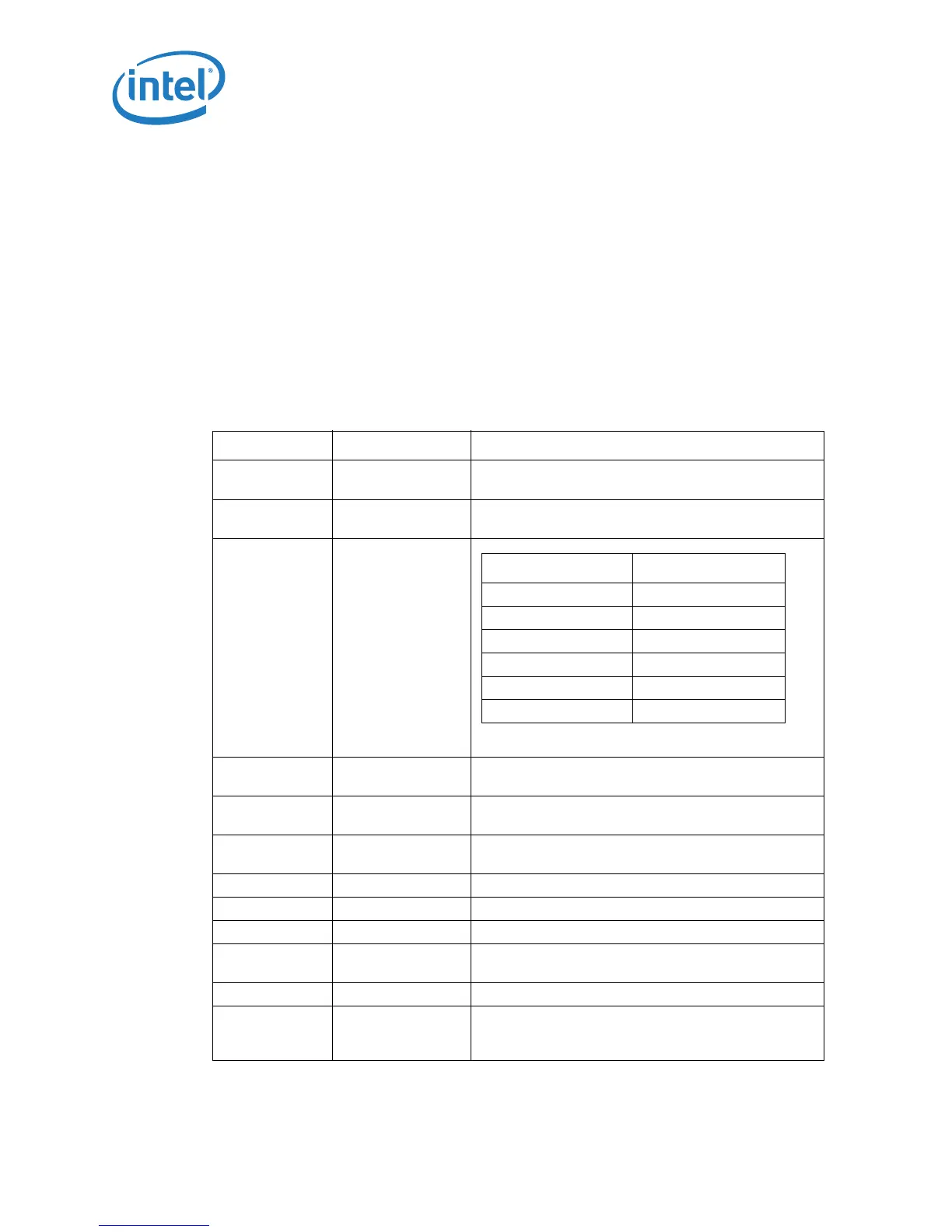
Tabl e 4 identifies which signals are common clock, source synchronous, and
asynchronous.
NOTES:See next page
Table 4. FSB Pin Groups
Signal Group Type Signals
1
AGTL+ Common
Clock Input
Synchronous to
BCLK[1:0]
BPRI#, DEFER#, PREQ#
5
, RESET#, RS[2:0]#, TRDY#
AGTL+ Common
Clock I/O
Synchronous to
BCLK[1:0]
ADS#, BNR#, BPM[3:0]#
3
, BR0#, DBSY#, DRDY#,
HIT#, HITM#, LOCK#, PRDY#
3
, DPWR#
AGTL+ Source
Synchronous
I/O
Synchronous to
assoc. strobe
AGTL+ Strobes
Synchronous to
BCLK[1:0]
ADSTB[1:0]#, DSTBP[3:0]#, DSTBN[3:0]#
CMOS Input Asynchronous
A20M#, DPRSTP#, DPSLP#, IGNNE#, INIT#, LINT0/
INTR, LINT1/NMI, PWRGOOD, SMI#, SLP#, STPCLK#
Open Drain
Output
Asynchronous FERR#, IERR#, THERMTRIP#
Open Drain I/O Asynchronous PROCHOT#
4
CMOS Output Asynchronous PSI#, VID[6:0], BSEL[2:0]
CMOS Input Synchronous to TCK TCK, TDI, TMS, TRST#
Open Drain
Output
Synchronous to TCK TDO
FSB Clock Clock BCLK[1:0]
Power/Other
COMP[3:0], DBR#
2
, GTLREF, RSVD, TEST2, TEST1,
THERMDA, THERMDC, V
CC
, V
CCA
, V
CCP
, V
CC_SENSE
,
V
SS
, V
SS_SENSE
Signals Associated Strobe
REQ[4:0]#, A[16:3]# ADSTB[0]#
A[35:17]# ADSTB[1]#
D[15:0]#, DINV0# DSTBP0#, DSTBN0#
D[31:16]#, DINV1# DSTBP1#, DSTBN1#
D[47:32]#, DINV2# DSTBP2#, DSTBN2#
D[63:48]#, DINV3# DSTBP3#, DSTBN3#