Package Mechanical Specifications and Pin Information
94 Datasheet
BPRI# Input
BPRI# (Bus Priority Request) is used to arbitrate for ownership of
the FSB. It must connect the appropriate pins of both FSB agents.
Observing BPRI# active (as asserted by the priority agent) causes
the other agent to stop issuing new requests, unless such requests
are part of an ongoing locked operation. The priority agent keeps
BPRI# asserted until all of its requests are completed, then releases
the bus by deasserting BPRI#.
BR0#
Input/
Output
BR0# is used by the processor to request the bus. The arbitration is
done between the processor (Symmetric Agent) and GMCH (High
Priority Agent).
BSEL[2:0] Output
BSEL[2:0] (Bus Select) are used to select the processor input clock
frequency. Tabl e 3 defines the possible combinations of the signals
and the frequency associated with each combination. The required
frequency is determined by the processor, chipset and clock
synthesizer. All agents must operate at the same frequency.
COMP[3:0] Analog
COMP[3:0] must be terminated on the system board using
precision (1% tolerance) resistors.
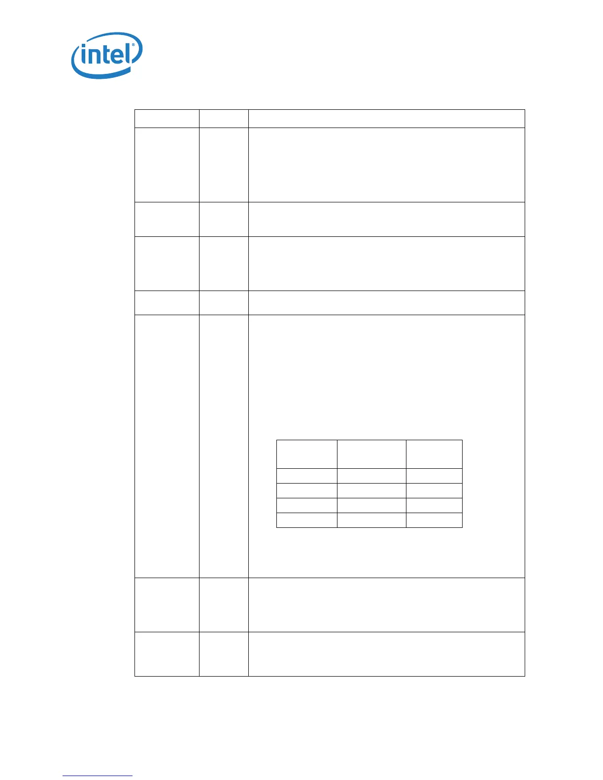
D[63:0]#
Input/
Output
D[63:0]# (Data) are the data signals. These signals provide a
64-bit data path between the FSB agents, and must connect the
appropriate pins on both agents. The data driver asserts DRDY# to
indicate a valid data transfer.
D[63:0]# are quad-pumped signals and will thus be driven four
times in a common clock period. D[63:0]# are latched off the
falling edge of both DSTBP[3:0]# and DSTBN[3:0]#. Each group of
16 data signals correspond to a pair of one DSTBP# and one
DSTBN#. The following table shows the grouping of data signals to
data strobes and DINV#.
Furthermore, the DINV# pins determine the polarity of the data
signals. Each group of 16 data signals corresponds to one DINV#
signal. When the DINV# signal is active, the corresponding data
group is inverted and therefore sampled active high.
DBR# Output
DBR# (Data Bus Reset) is used only in processor systems where no
debug port is implemented on the system board. DBR# is used by a
debug port interposer so that an in-target probe can drive system
reset. If a debug port is implemented in the system, DBR# is a no
connect in the system. DBR# is not a processor signal.
DBSY#
Input/
Output
DBSY# (Data Bus Busy) is asserted by the agent responsible for
driving data on the FSB to indicate that the data bus is in use. The
data bus is released after DBSY# is deasserted. This signal must
connect the appropriate pins on both FSB agents.
Table 19. Signal Description (Sheet 2 of 8)
Name Type Description
Quad-Pumped Signal Groups
Data Group
DSTBN#/
DSTBP#
DINV#
D[15:0]# 0 0
D[31:16]# 1 1
D[47:32]# 2 2
D[63:48]# 3 3