Quad-Core Intel® Xeon® Processor 5300 Series Datasheet 77
Land Listing
M27 VCC Power/Other
M28 VCC Power/Other
M29 VCC Power/Other
M3 STPCLK# CMOS
Asynchronous
Input
M30 VCC Power/Other
M4 A07# Source Sync Input/Output
M5 A03# Source Sync Input/Output
M6 REQ2# Source Sync Input/Output
M7 VSS Power/Other
M8 VCC Power/Other
N1 PWRGOOD CMOS
Asynchronous
Input
N2 IGNNE# CMOS
Asynchronous
Input
N23 VCC Power/Other
N24 VCC Power/Other
N25 VCC Power/Other
N26 VCC Power/Other
N27 VCC Power/Other
N28 VCC Power/Other
N29 VCC Power/Other
N3 VSS Power/Other
N30 VCC Power/Other
N4 A36# Source Sync Input/Output
N5 RESERVED
N6 VSS Power/Other
N7 VSS Power/Other
N8 VCC Power/Other
P1 TESTHI10 Power/Other Input
P2 SMI# CMOS
Asynchronous
Input
P23 VSS Power/Other
P24 VSS Power/Other
P25 VSS Power/Other
P26 VSS Power/Other
P27 VSS Power/Other
P28 VSS Power/Other
P29 VSS Power/Other
P3 INIT# CMOS
Asynchronous
Input
P30 VSS Power/Other
P4 VSS Power/Other
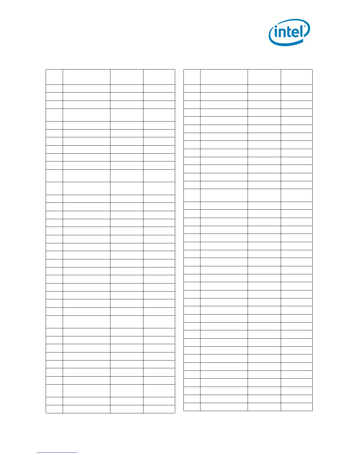
Table 4-2. Land Listing by Land Number
(Sheet 17 of 20)
Pin
No.
Pin Name
Signal
Buffer Type
Direction
P5 A37# Source Sync Input/Output
P6 A04# Source Sync Input/Output
P7 VSS Power/Other
P8 VCC Power/Other
R1 COMP3 Power/Other Input
R2 VSS Power/Other
R23 VSS Power/Other
R24 VSS Power/Other
R25 VSS Power/Other
R26 VSS Power/Other
R27 VSS Power/Other
R28 VSS Power/Other
R29 VSS Power/Other
R3 FERR#/PBE# Open Drain
Asynchronous
Output
R30 VSS Power/Other
R4 A08# Source Sync Input/Output
R5 VSS Power/Other
R6 ADSTB0# Source Sync Input/Output
R7 VSS Power/Other
R8 VCC Power/Other
T1 COMP1 Power/Other Input
T2 RESERVED
T23 VCC Power/Other
T24 VCC Power/Other
T25 VCC Power/Other
T26 VCC Power/Other
T27 VCC Power/Other
T28 VCC Power/Other
T29 VCC Power/Other
T3 VSS Power/Other
T30 VCC Power/Other
T4 A11# Source Sync Input/Output
T5 A09# Source Sync Input/Output
T6 VSS Power/Other
T7 VSS Power/Other
T8 VCC Power/Other
U1 TESTIN2 Power/Other Input
U2 AP0# Common Clk Input/Output
U23 VCC Power/Other
U24 VCC Power/Other
Table 4-2. Land Listing by Land Number
(Sheet 18 of 20)
Pin
No.
Pin Name
Signal
Buffer Type
Direction