Goodrive35 Series Closed-loop Vector Control VFD Basic operation instruction
190
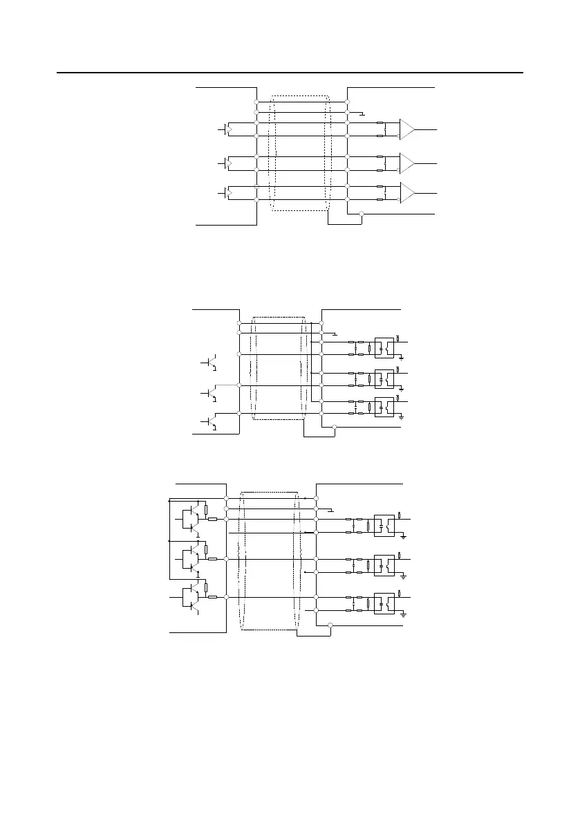
B+
A+
B -
B +
A -
A +
GND
5V
PE
VCC
0 V
A-
B-
A
Use shield cables
Differential
output
Z -
Z+
Z+
Z-
B
Z
Note: The diagram of differential output is given to the H1 interface, C1 interface applies opto-isolator
and H2 interface applies differential chips. The external wiring is the same as that of H1.
2. Open collector output (suitable to C1 and H1)
B -
B +
A -
A +
+5V
Open collector output
Use shield cables
B
A
+5V
OV
OV
B
A
0 V
VCC
PE
PWR/+12V
COM1/COM
Z -
Z +
+5V
Z
OV
Z
3. Complementary output (suitable to C1 and H1)
B -
B +
A -
A +
+5V
Use shield cables
B
A
+5V
B
A
0 V
VCC
PE
PWR/+12V
COM/COM1
Z -
Z +
+5V
Z
Z
OV
OV
OV
Note:
Above diagram are given to the features of common encoder and suitable to H1 interface.
The diagram of differential output is given to the H1 interface, C1 interface applies opto-isolator and
H2 interface applies differential chips. The external wiring is the same as that of H1.
If the external current is limited, C1and H1 interface is suitable to encoder signal and pulse reference
signal input with greater voltage.
 Loading...