Troubleshooting Tables: List of Board and IC Signals 7-47
mortable Specifies Mobile or
Portable hardware
W13 0=Porta-
ble
Input None 0 Output
gcai_gpio3 GPIO3 AA15 Input None 0 Output
gcai_gpio4 GPIO4 R14 Input None Input Pull-
down
bluetooth_ptt PTT signal from Blue-
tooth AVR
Y5 0=Pressed Input Pul-
lup
Input Pull-
down
f2_timer_input_ca
pture
"Receives one of
three timing signals
mux'ed through
CPLD - Abacus Sync,
DMCS, Ramp DAC
Trigger.
"P20 Input Pull-
down
Input Pull-
down
bt_avr_status AVR status read by
OMAP
P18 Input Pul-
lup
Input Pull-
down
enc_wakeup MACE encryption
wakeup
A6 1 Output 1 Output
enc_reset MACE encryption
reset
B6 0 I/O Pul-
lup
1 I/O Pul-
lup
5V_pwm_en Forces SW5 to PWM P14 1 Output Pul-
lup
0 Output Pul-
lup
gcai_gpio2 GPIO2 C13 Input None Input None
gcai_gpio1 GPIO1 C11 Input None Input None
gcai_gpio0 GPIO0 M7 Input None Input None
gcai_vbus_i_limit Current limit select for
GCAI VBUS
C6 1=500mA Output 0 Output
f2_paramp_mon Factory use to test F2
transmit timing.
Allows TX/RX signal
to appear on GCAI
GPIO3.
C5 1=Factory
Test
Output Pul-
lup
0 Output Pul-
lup
top_disp_data_ctrl Select for data or
control on top dis-
play(Not Used in
WWP)
P12 1=data Output 0 Output
top_display_reset Reset for color front
display( Not Used in
WWP)
M12 0 Output 1 Output
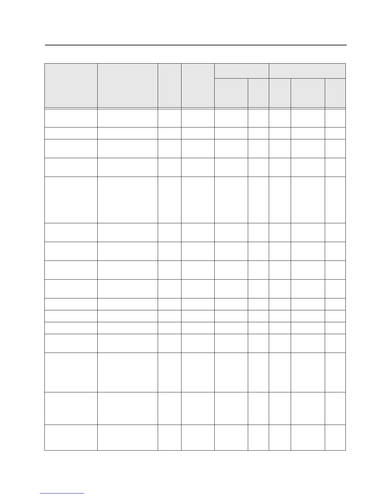
Table 7-18. Overall GPIO pin functions (Continued)
Signal Name Description
Pin
or
Ball #
Active
State
SW Initialized HW Reset
Direction
*
PU State Direction
*
PU
or
PD
 Loading...