Troubleshooting Tables: List of Board and IC Signals 7-53
Note:
* PU = Pull Up
* PD = Pull Down
** = Not applicable to APX 2000/ APX 4000 (Two Knobs)
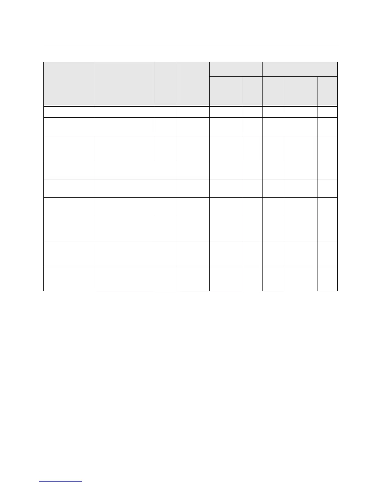
sda I2C Data V20 I/O None Input None
rtck JTAG Clock from
Controller
Y17 I/O None U Unknown None
tck JTAG Clock from
JTAG box to Control-
ler
W18 Input None Input Pull-
down
ntrst JTAG Reset from
JTAG box
Y18 Input None Input
omap_tms JTAG Test Mode
Select from JTAG box
V17 Input Input Pull-
down
omap_tdo JTAG Data out from
Controller
AA19 Output 0 Output None
tdi JTAD Data in from
JTAG box to Control-
ler
Y19 Input Input Pull-
down
nemu0 "Emulation pin 0, not
used, pulled high on
PCB
"V16 I/O Input Pul-
lup
nemu1 "Emulation pin 1, not
used, pulled high on
PCB
"W17 I/O Input Pul-
lup
Table 7-18. Overall GPIO pin functions (Continued)
Signal Name Description
Pin
or
Ball #
Active
State
SW Initialized HW Reset
Direction
*
PU State Direction
*
PU
or
PD
 Loading...