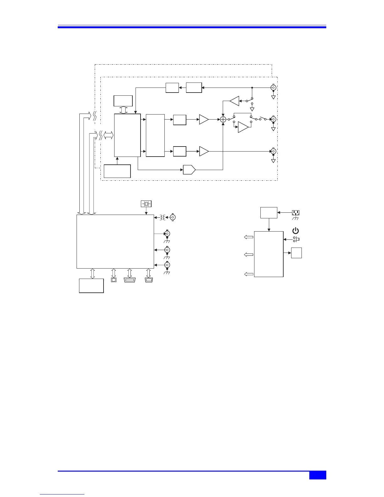
1.2 Operating Principles
3
WF1973/WF1974
■ WF1974 block diagram
• The analog block is insulated from the system controller block located in the housing
potential.
• In the WF1974, the analog block comprises two channels, each individually isolated from
the housing potential.
■ System controller block
• This block performs control of the analog block, including the display, panel key
processing, remote control (GPIB, USB) processing, trigger input processing, frequency
reference control, DDS control, amplitude, and DC offset.
• A 20 MHz crystal oscillator is used as the basic oscillation of the DDS.
• The signal to synchronize multiple units is sent to REF OUT (frequency reference output),
and the inter-channel sync (WF1974 only) is sent to the analog block of each channel.
■ Power supply block
• The AC/DC directly connected to the power supply input is in a constantly powered state.
• Control of each power supply circuit is done through power switch manipulation.
ANALOG CH1
AC/DC
FA N
for ANALOG CH1
+12V
㨪LINE
100V...230V
for ANALOG CH2
REF OUT
TRIG IN CH1
10MHz REF IN
TRIG IN CH2
ANALOG CH2
MOD/ADD
IN
FCTN
OUT
SYNC/SUB
OUT
A/D
LPF
LPF
DDS
D/A
DC OFFSET
16bit
512Kw
WAV E
MEMORY
120MHz
r10Vmax
PGA
0/-10/-20/-30dB
LPF
r1V
2
TTL/r3V
5
r2Vmax
EXTERNAL
MODULATION
EXTERNAL
ADDITION
ISOLATION
POWER
SUPPLY
for SYSTEM
CONTROLLER
20MHz
SYSTEM
CONTROLLER
MULTI
I/O
GPIBUSB
FRONT
PA N E L
UNIT
16bit-
2CH
D/A
CLOCK
GENERATOR