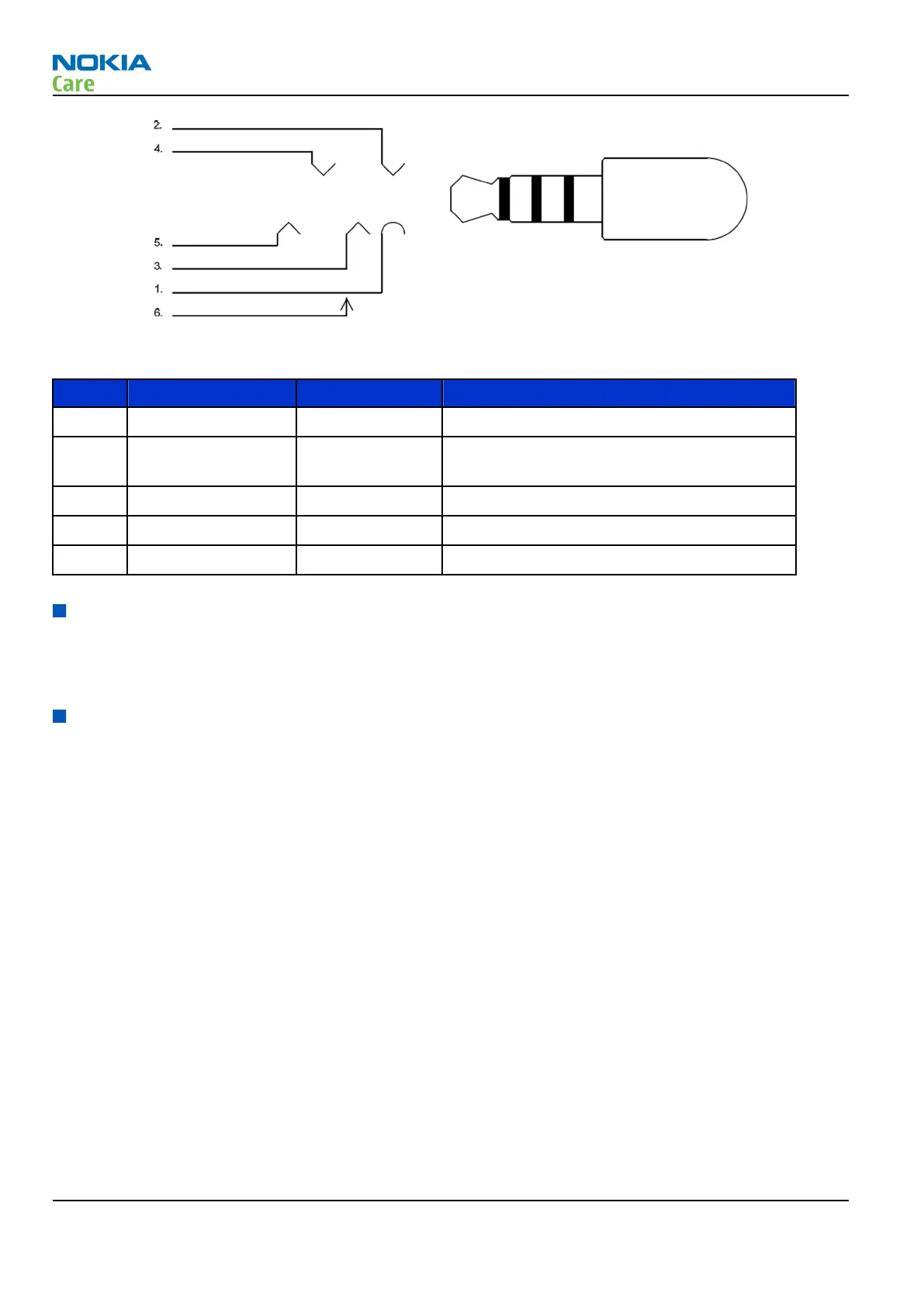
Figure 37 AV connector pin layout
Table 12 AV connector pins
Pin Signal name Direction Description
1, 2 HS_ GND - Ground contacts
3 HS_MIC Input Multiplexed microphone audio and control
data/muxed: MIC2P and ACI
4 HS_EAR_R Output Audio output (XEAR_R)
5 HS_EAR_L Output Audio output (XEAR_L)
6 PLUG_DET Input Terminal internal connection, plug detection
Combo memory
The die stacked combo memory module POP2 (1Gbit M3/ DDR SDRAM 512 Mbit) is assembled on the top of
RAP3GS2v4, and located at the bottom side of the main board. RAP3GS2v4 has pads on the top of it, where
POP2 is soldered. These components cannot be replaced. The engine module must be replaced.
RF description
Receiver (RX)
An analogue signal is received by the phone's antenna. The signal is converted to a digital signal and is then
transferred further to the baseband (e.g. to the earpiece).
The receiver functions are implemented in the RF ASIC.
Signals with different frequencies take different paths, therefore being handled by different components.
The principle of GSM and WCDMA is the same.
Transmitter (TX)
The digital baseband signal (e.g. from the microphone) is converted to an analogue signal, which is then
amplified and transmitted from the antenna. The frequency of this signal can be tuned to match the bandwith
of the system in use (e.g. GSM900).
The transmitter functions are implemented in the RF ASIC.
Even though the GSM and WCDMA signals are sent via different components, the principle of the transmission
is the same.
RM-721; RM-722
System Module
Page 5 – 20 COMPANY CONFIDENTIAL Issue 1
Copyright © 2011 Nokia. All rights reserved.