4.1 What the Link2 boot LED indicates
LED D10 is the Link2 MCU BOOT0_LED indicator. This LED reflects the state of Link2
MCU pin P1_1. When the boot process fails, D1 will toggle at a 1 Hz rate for 60
seconds. After 60 seconds, the Link2 MCU is reset.
4.2 Programming the Link2 firmware
As mentioned earlier in this section, it is not normally necessary to program the Link2
firmware. However, this can easily be accomplished using the supporting utility,
LPCScrypt.
To program the Link2 Flash the Link2 device (LPC432x) must be in DFU mode. If the
Link2 already has a valid image in the flash, it will need to be forced into DFU mode by
placing a jumper shunt on JP5, and power cycling (disconnecting then reconnecting
power via J8.) Link2 MCU programming is performed using the LPCScrypt utility (see
http://www.nxp.com/lpcutilities). Instructions for using the tool are located at the same
web page.
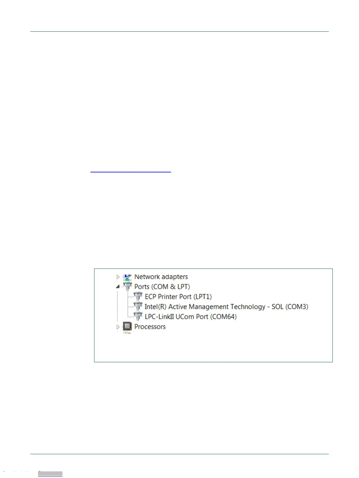
4.3 VCOM port
The identifier of the VCOM port will vary between boards and hosts. To determine the
COM port, open the Windows operating system Device Manager. This can be achieved
by going to the Windows operating system Start menu and typing “Device Manager” in
the search bar. In the device manager look under “Ports”; the LPC-LinkII UCom Port
device and its name should be visible. NOTE: this VCOM port will only appear if (a) the
Debug Probe has been programmed with the CMSIS-DAP firmware and the Debug
Probe DFU link is removed at power up, or (b) if the Debug Probe has been configured
for DFU boot (JP5 installed) at power up and MCUXpresso IDE has booted it (by starting
a debug session.)
If the J-Link firmware image has been programmed into the Debug Probe and DFU boot
mode is not being used, then a VCOM device called Jlink CDC UART port will appear
instead of the LPC-LinkII UCom port.

 Loading...


