EasyManua.ls Logo

Panasonic SA-PT480PH

Panasonic SA-PT480PH
162 pages
To Next Page IconTo Next Page
Loading...
© Panasonic Corporation 2010. All rights reserved.
Unauthorized copying and distribution is a violation
of law.
PSG1004020CE
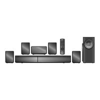
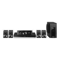
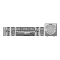
DVD Home Theater Sound System
Model No. SA-PT480PH
Product Color: (K)...Black Type
TABLE OF CONTENTS
PAGE PAGE
1 Safety Precautions----------------------------------------------- 3
1.1. GENERAL GUIDELINES-------------------------------- 3
1.2. Before Use -------------------------------------------------- 3
1.3. Before Repair and Adjustment ------------------------- 3
1.4. Protection Circuitry---------------------------------------- 5
1.5. Safety Parts Information --------------------------------- 5
2 Warning-------------------------------------------------------------- 6
2.1. Prevention of Electrostatic Discharge (ESD)
to Electrostatic Sensitive (ES) Devices -------------- 6
2.2. Precaution of Laser Diode------------------------------- 7
2.3. Service caution based on Legal restrictions-------- 8
2.4. Handling Precautions for Traverse Unit-------------- 9
3 Service Navigation----------------------------------------------11
3.1. Service Information-------------------------------------- 11
4 Specifications---------------------------------------------------- 12
5 Location of Controls and Components------------------ 14
5.1. Remote Control Key Button Operations------------ 14
5.2. Main Unit Key Button Operations-------------------- 15
5.3. Speaker Connection------------------------------------- 15
5.4. Using the VIERA Link “HDAVI Control™”---------- 16
5.5. Using of iPod/iPhone------------------------------------ 18
5.6. Disc Information ------------------------------------------ 19
6 Self-Diagnostic and Special Mode Setting ------------- 21
6.1. Cold-Start -------------------------------------------------- 21
6.2. Service Mode Table ------------------------------------- 21
6.3. Self-Diagnostic Mode ----------------------------------- 27
Note: Please refer to the original service manual for:
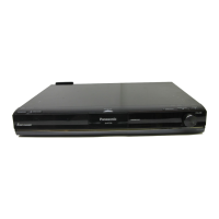
O DVD Mechanism Unit (DLS6E), Order No. PSG0909002AE
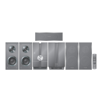
O Speaker system SB-PT480P-K, Order No. PSG0912003CE

Table of Contents

Questions and Answers:

Panasonic SA-PT480PH Specifications

General IconGeneral
Total Power Output1000W
Speaker Configuration5.1 Channel
USB PlaybackYes
HDMI Output1
TypeHome Theater System
Surround Sound FormatsDolby Digital, DTS

Summary

1 Safety Precautions

1.1 General Guidelines

General guidelines for servicing, including lead dress, protective devices, and leakage current checks.

1.2 Before Use

Instruction to disconnect mains cord before adjusting voltage selector.

1.3 Before Repair and Adjustment

Procedures and cautions before repair, including capacitor discharge.

1 Safety Precautions

1.3.1 Caution for Fuse Replacement

Caution to replace fuses only with the same type.

1 Safety Precautions

1.4 Protection Circuitry

Information about protection circuitry operation and troubleshooting.

1.5 Safety Parts Information

List of critical safety parts and importance of using manufacturer-specified parts.

2 Warning

2.1 Prevention of Electrostatic Discharge (ESD)

Techniques to reduce component damage from static electricity during handling.

2 Warning

2.2 Precaution of Laser Diode

Cautions regarding laser radiation exposure and handling of the laser diode pickup unit.

2 Warning

2.3 Service Caution Based on Legal Restrictions

Description of lead-free solder (PbF) and service cautions for repair work.

2 Warning

2.4 Handling Precautions for Traverse Unit

Cautions for handling the traverse unit, especially the optical pickup and laser diode.

2.4.1 Cautions for Optical Pickup Unit Handling

Specific precautions for handling the optical pickup unit to prevent ESD damage.

2.4.2 Grounding for Electrostatic Breakdown Prevention

Importance of grounding and worktable grounding procedures.

2 Warning

2.4.2.2 Human Body Grounding

Procedure using an anti-static wrist strap to discharge static electricity.

3 Service Navigation

3.1 Service Information

Information about the service manual's content and ordering parts.

4 Specifications

General Specifications

General specifications like power supply, dimensions, mass, operating conditions.

Amplifier Section Specifications

Specifications for RMS Output Power and PMPO Output Power in Dolby Digital mode.

FM Tuner & Terminals Specifications

Specifications for FM tuner presets, frequency range, antenna terminals, digital audio input, and mic jack.

Disc Section Specifications

Information about playable discs, file format support, and picture resolution.

5 Location of Controls and Components

5.1 Remote Control Key Button Operations

Explanation of key button functions on the remote control for various operations.

5 Location of Controls and Components

5.2 Main Unit Key Button Operations

Explanation of key button functions on the main unit for various operations.

5.3 Speaker Connection

Guidance on connecting speakers, paying attention to color and polarity.

5 Location of Controls and Components

5.4 Using the VIERA Link HDAVI Control

Features and operation of VIERA Link for connected AV equipment control via HDMI.

5 Location of Controls and Components

Speaker Selection

How to select audio output and control speaker behavior based on input and mode.

TV Speaker Activation

How TV speakers are activated and audio output is selected.

5 Location of Controls and Components

5.5 Using of iPodiPhone

Instructions for connecting and using iPod/iPhone, including playback controls and charging.

5 Location of Controls and Components

5.6 Disc Information

Details on playable media formats and disc playability.

5.6.1 Disc Playability (Media)

Information on commercial discs and recorded discs, including handling precautions.

5 Location of Controls and Components

5.6.2 File Extension Type Support

Supported file extensions for WMA, MP3, JPEG, MPEG4, and DivX formats.

6 Self-Diagnostic and Special Mode Setting

6.1 Cold-Start

Procedure to initialize the unit to shipping mode by unplugging and pressing the power button.

6.2 Service Mode Table

Information on activating service modes via button combinations on the main unit and remote control.

6 Self-Diagnostic and Special Mode Setting

6.2.1 Service Mode Table 1 (For DVD)

Details on error code check, jitter check, and initial laser drive current setting.

6 Self-Diagnostic and Special Mode Setting

6.2.2 Service Mode Table 2 (For DVD)

Information on DVD laser drive current measurement, region display, and CPPM/CPRM keys check.

6 Self-Diagnostic and Special Mode Setting

6.2.4 Service Mode Table 4 (For DVD)

Details on DVD firmware version display, timer checks, and spindle motor operation timer reset.

6 Self-Diagnostic and Special Mode Setting

6.3 Self-Diagnostic Mode

Procedures for entering self-diagnostic mode and checking/clearing error codes.

6 Self-Diagnostic and Special Mode Setting

6.4.1 Mechanism Error Code Table (DLS6 E)

Table listing mechanism error codes, diagnosis contents, and automatic FL display.

6 Self-Diagnostic and Special Mode Setting

6.4.2 DVD Module Error Code Table

Table listing DVD module error codes related to HDMI communication and firmware.

6 Self-Diagnostic and Special Mode Setting

6.4.3 Power Supply & Digital Amplifier Error Code Table

Error codes F61 and F76 related to power supply and digital amplifier issues.

6 Self-Diagnostic and Special Mode Setting

6.5 Sales Demonstration Lock Function

Function to prevent disc ejection and operation for sales demonstrations.

6.5.1 Setting

Procedure to prohibit disc removal and operation by locking the unit.

6.5.2 Cancellation

Procedure to cancel the sales demonstration lock function.

6 Self-Diagnostic and Special Mode Setting

6.6 Firmware Version-Up Information

Information and process flow for updating the unit's firmware.

6.6.1 Process Flow (13)

Steps for collecting ROM files, loading the disc, and initiating the update process.

6 Self-Diagnostic and Special Mode Setting

6.6.2 Process Flow (23)

Process flow for checking ROM file types and update necessity.

7 Troubleshooting Guide

7.1 Troubleshooting Guide for F61 andor F76

Checking procedures for error codes F61 and F76 related to SMPS P.C.B. faults.

7 Troubleshooting Guide

7.2 Part Location

Illustration showing the location of key components on the SMPS P.C.B.

7 Troubleshooting Guide

7.3 Basic Troubleshooting Guide for Traverse Unit (Main P.C.B.)

Troubleshooting steps for common problems with the traverse unit and main P.C.B.

7 Troubleshooting Guide

7.4 Basic Troubleshooting Guide for HDMI AV output

Troubleshooting steps for HDMI AV output issues like no display or audio.

7 Troubleshooting Guide

HDMI AV Output Troubleshooting Continuation

Further troubleshooting steps for HDMI AV output problems like blank display or color issues.

8 Disassembly and Assembly Instructions

Caution Note

General cautions regarding disassembly and assembly procedures, tools, and handling.

8 Disassembly and Assembly Instructions

8.1 Disassembly Flow Chart

Visual flow chart illustrating the sequence of disassembly for various unit components.

8 Disassembly and Assembly Instructions

8.2 Main Components and P.C.B. Locations

Diagram showing the location of major components and printed circuit boards within the unit.

8 Disassembly and Assembly Instructions

8.3 Disassembly of Top Cabinet

Step-by-step procedure for removing the top cabinet of the unit.

8 Disassembly and Assembly Instructions

8.4 Disassembly of AC Inlet P.C.B.

Procedure for removing the AC inlet printed circuit board.

8.5 Disassembly of Voltage Selector P.C.B.

Procedure for removing the voltage selector printed circuit board.

8 Disassembly and Assembly Instructions

8.6 Disassembly of Rear Panel

Procedure for removing the rear panel of the unit.

8.7 Disassembly of DVD Mechanism Unit (DLS6 E)

Procedure for removing the DVD mechanism unit from the main unit.

8 Disassembly and Assembly Instructions

Assembly of DVD Mechanism Unit (DLS6 E)

Procedure for installing the DVD mechanism unit back into the unit.

8 Disassembly and Assembly Instructions

8.8 Disassembly of Front Panel Block Assembly

Step-by-step procedure for removing the front panel block assembly.

8 Disassembly and Assembly Instructions

8.9 Disassembly of FL P.C.B.

Procedure for removing the FL (Fluorescent Display) printed circuit board.

8 Disassembly and Assembly Instructions

Assembly of FL P.C.B.

Procedure for installing the FL printed circuit board back into the unit.

8.10 Disassembly of Power Button P.C.B.

Procedure for removing the power button printed circuit board.

8 Disassembly and Assembly Instructions

Assembly of Power Button P.C.B.

Procedure for installing the power button printed circuit board.

8 Disassembly and Assembly Instructions

8.11 Replacement of Cradle Lid

Procedure for replacing the cradle lid, including disassembly steps.

8.11.1 Disassembly of Cradle Lid

Steps for disassembling the cradle lid.

8 Disassembly and Assembly Instructions

8.11.2 Assembly of Cradle Lid

Procedure for assembling the cradle lid onto the front panel.

8 Disassembly and Assembly Instructions

8.12 Disassembly of iPod Cradle Assembly

Procedure for removing the iPod cradle assembly.

8 Disassembly and Assembly Instructions

Assembly of iPod Cradle Assembly

Procedure for fixing the iPod cradle assembly to the front panel.

8 Disassembly and Assembly Instructions

8.13 Disassembly of iPodiPhone P.C.B.

Procedure for removing the iPod/iPhone printed circuit board.

8 Disassembly and Assembly Instructions

8.14 Disassembly of USB P.C.B.

Procedure for removing the USB printed circuit board.

8.15 Disassembly of Mic P.C.B.

Procedure for removing the microphone printed circuit board.

8 Disassembly and Assembly Instructions

8.16 Replacement of DVD Lid Unit

Procedure for replacing the DVD lid unit, including disassembly steps.

8.16.1 Disassembly of DVD Lid Unit

Steps for disassembling the DVD lid unit.

8 Disassembly and Assembly Instructions

8.16.2 Assembly of DVD Lid Unit

Procedure for assembling the DVD lid unit into the front panel.

8 Disassembly and Assembly Instructions

8.17 Disassembly of Front Shield Unit

Procedure for removing the front shield unit.

8 Disassembly and Assembly Instructions

8.18 Disassembly of Main P.C.B.

Step-by-step procedure for removing the main printed circuit board.

8 Disassembly and Assembly Instructions

Main P.C.B. Shield Unit Removal

Steps for lifting and removing the main P.C.B. shield unit.

8 Disassembly and Assembly Instructions

8.19 Disassembly of D-Amp P.C.B.

Procedure for removing the D-Amp (Digital Amplifier) printed circuit board.

8 Disassembly and Assembly Instructions

8.20 Replacement of Digital Amplifier IC (IC5100 IC5200)

Procedure for replacing the digital amplifier ICs, including disassembly steps.

8.20.1 Disassembly of Digital Amplifier IC (IC5100 IC5200)

Steps for disassembling the digital amplifier ICs.

8 Disassembly and Assembly Instructions

8.20.2 Assembly of Digital Amplifier IC (IC5100 IC5200)

Procedure for assembling the digital amplifier ICs onto the D-Amp P.C.B.

8.21 Disassembly of Power P.C.B.

Procedure for removing the power printed circuit board.

8 Disassembly and Assembly Instructions

8.22 Disassembly of SMPS P.C.B.

Procedure for removing the SMPS (Switch Mode Power Supply) printed circuit board.

8 Disassembly and Assembly Instructions

SMPS P.C.B. Removal

Detailed steps for removing the SMPS P.C.B., including releasing spacers and desoldering wires.

8 Disassembly and Assembly Instructions

8.23 Replacement of Switching Regulator IC (IC5701)

Procedure for replacing the switching regulator IC, including disassembly and assembly steps.

8.23.1 Disassembly of Switching Regulator IC (IC5701)

Steps for disassembling the switching regulator IC.

8 Disassembly and Assembly Instructions

8.24 Replacement of Rectifier Diode (D5702)

Procedure for replacing the rectifier diode, including disassembly and assembly steps.

8.24.1 Disassembly of Rectifier Diode (D5702)

Steps for disassembling the rectifier diode.

8 Disassembly and Assembly Instructions

8.24.2 Assembly of Rectifier Diode (D5702)

Procedure for assembling the rectifier diode onto the SMPS P.C.B.

8.25 Replacement of Regulator Diode (D5802)

Procedure for replacing the regulator diode, including disassembly and assembly steps.

8.25.1 Disassembly of Regulator Diode (D5802)

Steps for disassembling the regulator diode.

8 Disassembly and Assembly Instructions

8.25.2 Assembly of Regulator Diode (D5802)

Procedure for assembling the regulator diode onto the SMPS P.C.B.

8.26 Replacement of Regulator Diode (D5803)

Procedure for replacing the regulator diode, including disassembly and assembly steps.

8.26.1 Disassembly of Regulator Diode (D5803)

Steps for disassembling the regulator diode.

8 Disassembly and Assembly Instructions

8.26.2 Assembly of Regulator Diode (D5803)

Procedure for assembling the regulator diode onto the SMPS P.C.B.

8.27 Disassembly of Fan

Procedure for removing the cooling fan unit.

8 Disassembly and Assembly Instructions

Fan Unit Removal

Steps for removing the fan unit from the rear panel.

Fan Cover Removal

Steps for removing the fan cover to access the fan.

9 Assembling and Disassembling of Traverse Unit

9.1 Disassembly of Traverse Unit

Procedure for disassembling the traverse unit, referring to DVD mechanism unit instructions.

9.2 Assembly of Traverse Unit

Procedure for assembling the traverse unit into the chassis.

9 Assembling and Disassembling of Traverse Unit

Traverse Unit Slotting and Placement

Steps for slotting and placing the traverse unit into the mechanism chassis.

10 Service Position

10.1 Checking & Repairing Main P.C.B.

Steps for checking and repairing the main P.C.B., focusing on Side B.

10.1.1 Checking & Repairing of Side B of Main P.C.B.

Detailed steps for accessing and working on Side B of the main P.C.B.

10 Service Position

10.1.2 Checking & Repairing of Side A of Main P.C.B.

Steps for accessing and working on Side A of the main P.C.B.

10 Service Position

10.2 Checking & Repairing D-Amp P.C.B.

Procedures for checking and repairing the D-Amp P.C.B., focusing on Side B and Side A.

10.2.1 Checking & Repairing of Side B of D-Amp P.C.B.

Steps for accessing and working on Side B of the D-Amp P.C.B.

10 Service Position

10.2.2 Checking & Repairing of Side A of D-Amp P.C.B.

Steps for accessing and working on Side A of the D-Amp P.C.B.

10 Service Position

10.3 Checking & Repairing SMPS P.C.B.

Procedures for checking and repairing the SMPS P.C.B.

10 Service Position

SMPS P.C.B. Check and Repair

Detailed steps for checking and repairing the SMPS P.C.B.

10 Service Position

10.4 Checking & Repairing FL P.C.B.

Procedures for checking and repairing the FL printed circuit board.

11 Voltage & Waveform Chart

11.1 Main P.C.B. (17)

Table of voltage indication values for various points on the Main P.C.B.

11 Voltage & Waveform Chart

11.2 Main P.C.B. (27)

Table of voltage indication values for various points on the Main P.C.B.

11 Voltage & Waveform Chart

11.3 Main P.C.B. (37)

Table of voltage indication values for various points on the Main P.C.B.

11 Voltage & Waveform Chart

11.4 Main P.C.B. (47)

Table of voltage indication values for various points on the Main P.C.B.

11 Voltage & Waveform Chart

11.5 Main P.C.B. (57)

Table of voltage indication values for various points on the Main P.C.B.

11 Voltage & Waveform Chart

11.6 Main P.C.B. (67)

Table of voltage indication values for various points on the Main P.C.B.

11 Voltage & Waveform Chart

11.7 Main P.C.B. (77)

Table of voltage indication values for various points on the Main P.C.B.

11 Voltage & Waveform Chart

11.8 FL P.C.B.

Table of voltage indication values for points on the FL P.C.B.

11 Voltage & Waveform Chart

11.9 D-Amp P.C.B. (12)

Table of voltage indication values for points on the D-Amp P.C.B.

11 Voltage & Waveform Chart

11.10 D-Amp P.C.B. (22)

Table of voltage indication values for points on the D-Amp P.C.B.

11.11 SMPS P.C.B.

Table of voltage indication values for points on the SMPS P.C.B.

11.12 Power P.C.B.

Table of voltage indication values for points on the Power P.C.B.

11 Voltage & Waveform Chart

11.13 Mic P.C.B.

Table of voltage indication values for points on the Mic P.C.B.

11 Voltage & Waveform Chart

11.14 Waveform Table (13)

Visual representations of waveforms for various ICs, specifying voltage and time per division.

11 Voltage & Waveform Chart

11.15 Waveform Table (23)

Visual representations of waveforms for various ICs, specifying voltage and time per division.

11 Voltage & Waveform Chart

11.16 Waveform Table (33)

Visual representations of waveforms for various ICs, specifying voltage and time per division.

12 Illustration of ICs, Transistor and Diode

13 Overall Simplified Block Diagram

14 Block Diagram

14.1 Main(Servo)

Block diagram illustrating the servo system of the main unit.

14 Block Diagram

14.2 Main(System Control)

Block diagram of the main unit's system control, including micro-processor and peripheral circuits.

14 Block Diagram

14.3 Main(UP-CON)

Block diagram of the main unit's up-conversion circuit, including HDMI transmitter.

14 Block Diagram

14.4 Main(Audio)

Block diagram illustrating the audio signal path, including inputs and processing.

14 Block Diagram

Main Audio (22) Block Diagram

Continuation of the audio block diagram showing digital sound processor and echo circuit.

14 Block Diagram

14.5 Main(Video)

Block diagram showing the video signal path, including SDRAM and flash memory interfaces.

14 Block Diagram

14.6 Digital Audio

Block diagram detailing the digital audio signal processing and amplifier outputs.

14 Block Diagram

14.7 Analog Video

Block diagram illustrating the analog video signal path, including input and output stages.

14 Block Diagram

14.8 Power Supply (12)

Block diagram of the power supply unit, showing AC input, transformers, and regulators.

14 Block Diagram

Power Supply (22) Block Diagram

Continuation of the power supply block diagram, showing voltage regulators and control circuits.

15 Wiring Connection Diagram

16 Schematic Diagram Notes

17 Schematic Diagram

17.1 Main Circuit

Schematic of the main circuit, showing DV5U LSI and connections.

17 Schematic Diagram

Main Circuit Diagram 2

Continuation of the main circuit schematic, showing SDRAM and flash memory interfaces.

17 Schematic Diagram

Main Circuit Diagram 3

Continuation of the main circuit schematic, showing video drivers and signal lines.

17 Schematic Diagram

Main Circuit Diagram 4

Continuation of the main circuit schematic, showing memory interfaces and address/data buses.

17 Schematic Diagram

Main Circuit Diagram 5

Continuation of the main circuit schematic, detailing signal lines and interface connections.

17 Schematic Diagram

Main Circuit Diagram 6

Continuation of the main circuit schematic, showing USB interface and other connections.

17 Schematic Diagram

17.1 Main HDMI Circuit

Schematic of the main HDMI circuit, showing HDMI transmitter and related components.

17 Schematic Diagram

17.2 Main MICON Circuit

Schematic of the main MICON circuit, showing micro-controller and peripheral interfaces.

17 Schematic Diagram

Main MICON Circuit Continuation

Continuation of the MICON schematic, showing A/D converter and DSP interfaces.

17 Schematic Diagram

Main MICON Circuit Continuation 2

Further continuation of the MICON schematic, showing speaker output drivers.

17 Schematic Diagram

Main MICON Circuit Continuation 3

Further continuation of the MICON schematic, showing power supply and regulator sections.

17 Schematic Diagram

Main MICON Circuit Continuation 4

Further continuation of the MICON schematic, showing voltage regulators and DC detect circuits.

17 Schematic Diagram

Main MICON Circuit Continuation 5

Further continuation of the MICON schematic, showing echo processor and headphone output circuits.

17 Schematic Diagram

17.2 FL Circuit

Schematic of the FL circuit, showing the display driver IC and associated components.

17 Schematic Diagram

17.3 D-Amp Circuit

Schematic of the D-Amp circuit, showing digital amplifiers and PWM processors.

17 Schematic Diagram

D-Amp Circuit Continuation

Continuation of the D-Amp schematic, showing output stages and DC detect circuits.

17 Schematic Diagram

D-Amp Circuit Continuation 2

Further continuation of the D-Amp schematic, showing output stages and component connections.

17 Schematic Diagram

D-Amp Circuit Continuation 3

Further continuation of the D-Amp schematic, showing output stages and thermal protection components.

17 Schematic Diagram

17.4 SMPS Circuit

Schematic of the SMPS circuit, showing switching power supply control and transformers.

17 Schematic Diagram

SMPS Circuit Continuation

Continuation of the SMPS schematic, showing voltage regulators and feedback circuits.

17 Schematic Diagram

17.5 Power, Power Button & AC Inlet Circuit

Schematics for the power supply, power button, and AC inlet circuits.

17 Schematic Diagram

17.6 iPodiPhone, USB & Voltage Selector Circuit

Schematics for the iPod/iPhone, USB, and voltage selector circuits.

17 Schematic Diagram

17.7 Mic Circuit

Schematic of the microphone circuit, showing op-amps and echo processing.

18 Printed Circuit Board

18.1 Main P.C.B. (Side A)

Top-down view of the Main P.C.B. (Side A), showing component layout.

18 Printed Circuit Board

18.1 Main P.C.B. (Side B)

Top-down view of the Main P.C.B. (Side B), showing component layout.

18 Printed Circuit Board

18.2 FL, Power, Power Button & AC Inlet P.C.B.

Views of the FL, Power, Power Button, and AC Inlet PCBs.

18 Printed Circuit Board

18.3 D-Amp P.C.B.

Views of the D-Amp P.C.B. (Side A and Side B), showing component layout.

18 Printed Circuit Board

18.4 SMPS P.C.B.

Top-down view of the SMPS P.C.B., showing component layout.

18 Printed Circuit Board

18.5 iPodiPhone, USB, Voltage Selector & Mic P.C.B.

Views of the iPod/iPhone, USB, Voltage Selector, and Mic PCBs.

19 Terminal Function of ICs

19.1 IC2300 (RFKWMPT480 GA): IC MICROPROCESSOR

Terminal function description for the microprocessor IC, listing pins and their descriptions.

19 Terminal Function of ICs

19.2 IC6001 (C0 HBB0000057): IC FL Driver

Terminal function description for the FL driver IC, listing pins and their functions.

20 Exploded View and Replacement Parts List

20.1 Exploded View and Mechanical Replacement Part List

Exploded view diagram and list of mechanical replacement parts for cabinet components.

20.1.1 Cabinet Parts Location

Illustration showing the location of cabinet parts and their corresponding numbers.

20 Exploded View and Replacement Parts List

20.1.2 Packaging

Diagram showing the packaging of the unit and its accessories.

20 Exploded View and Replacement Parts List

20.1.3 Mechanical Replacement Part List

Detailed list of mechanical replacement parts with safety ref. numbers and descriptions.

20.2 Electrical Replacement Part List

Related product manuals