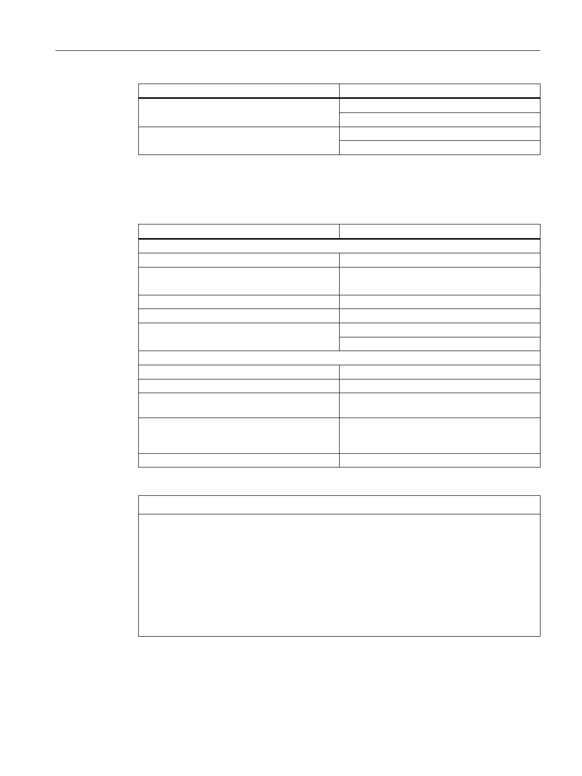
Parameters Values
Signal level (including ripple) High signal level: 15 V to 30 V
Low level: -3 V to 5 V
Input delay (typ.) L → H: 50 μs
H → L: 100 μs
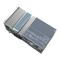
Digital inputs/outputs at X122 / X132 / X142
Table 7-30 Technical data of the digital inputs/outputs of X122 / X132 / X142
Parameters Values
As an input
Voltage -3 V to +30 V DC
Typical current consumption 9 mA at 24 V DC (only with NCU 710.3B)
2.5 mA at 24 V DC (only with NCU 720.3B/ 730.3B)
Signal level (including ripple) High signal level: 15 V to 30 V
Low level: -3 V to 5 V
Input delay (typ.) of inputs / "rapid inputs" L → H: 50 μs/5 μs
H → L: 100 μs / 50 μs
As an output
Voltage 24 V DC
Maximum load current per output 500 mA continuously short circuit-proof
Output delay (typ./max.)
1)
L → H: 150 μs / 400 μs
H → L: 75 μs / 100 μs
Switching frequency for resistive load: max. 100 Hz
for inductive load: max. 0.5 Hz
for lamp load: max. 10 Hz
max. lamp load 5 W
1)
Data for: V
cc
= 24 V; load 48 Ω; High = 90 % V
out
; Low = 10 % V
out
NOTICE
Ensuring the function of the digital inputs
An open input is interpreted as "low".
Only "rapid inputs" can be used as inputs for BEROs and probes.
Terminals G1 or G2 must be connected for the digital inputs to work. This can be done as
follows:
• Connect the ground reference of the digital inputs.
• A jumper to terminal M (note that these digital inputs are then no longer electrically
isolated).
Connecting
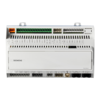
7.10 Digital inputs/outputs
NCU 7x0.3B PN
Equipment Manual, 10/2020, 6FC5397-1EP40-6BA1 81
 Loading...