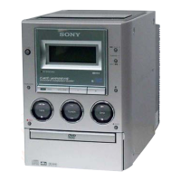
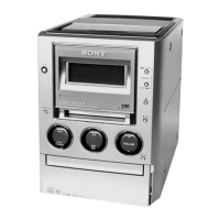
HCD-MD555
— 89 — — 90 —
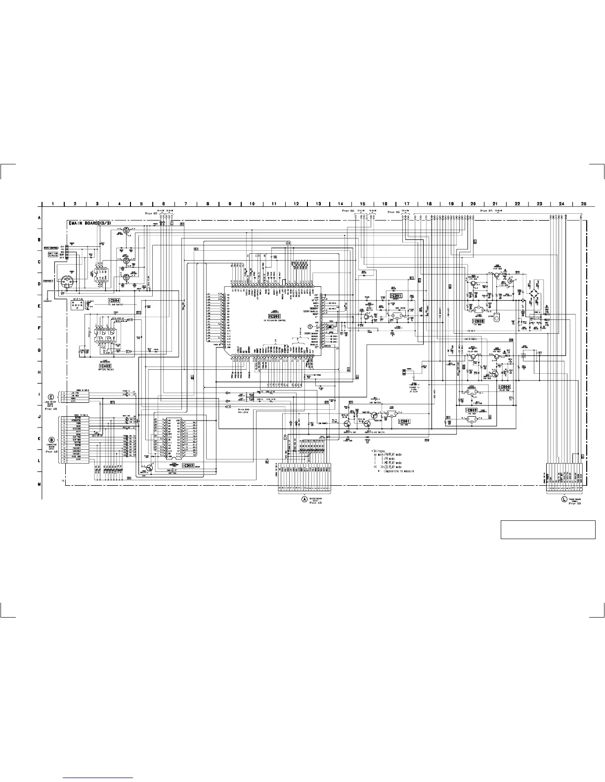
7-17. SCHEMATIC DIAGRAM — MAIN SECTION (3/3) —
• Refer to page 83 for Printed Wiring Board. • Refer to page 104 for Waveforms.
• Refer to page 109 for IC Block Diagrams. • Refer to page 121, 122 for IC Pin Function Description.
The components identified by mark ! or dotted
line with mark ! are critical for safety.
Replace only with part number specified.