C ircu it D escription—434
C hanne l 1 D iod e G ate
C U R R E N T PA T H
R E V E R S E -B IA S E D D IO D E S
V e rtica l
signal to
D e la y-L in e
D river Stage
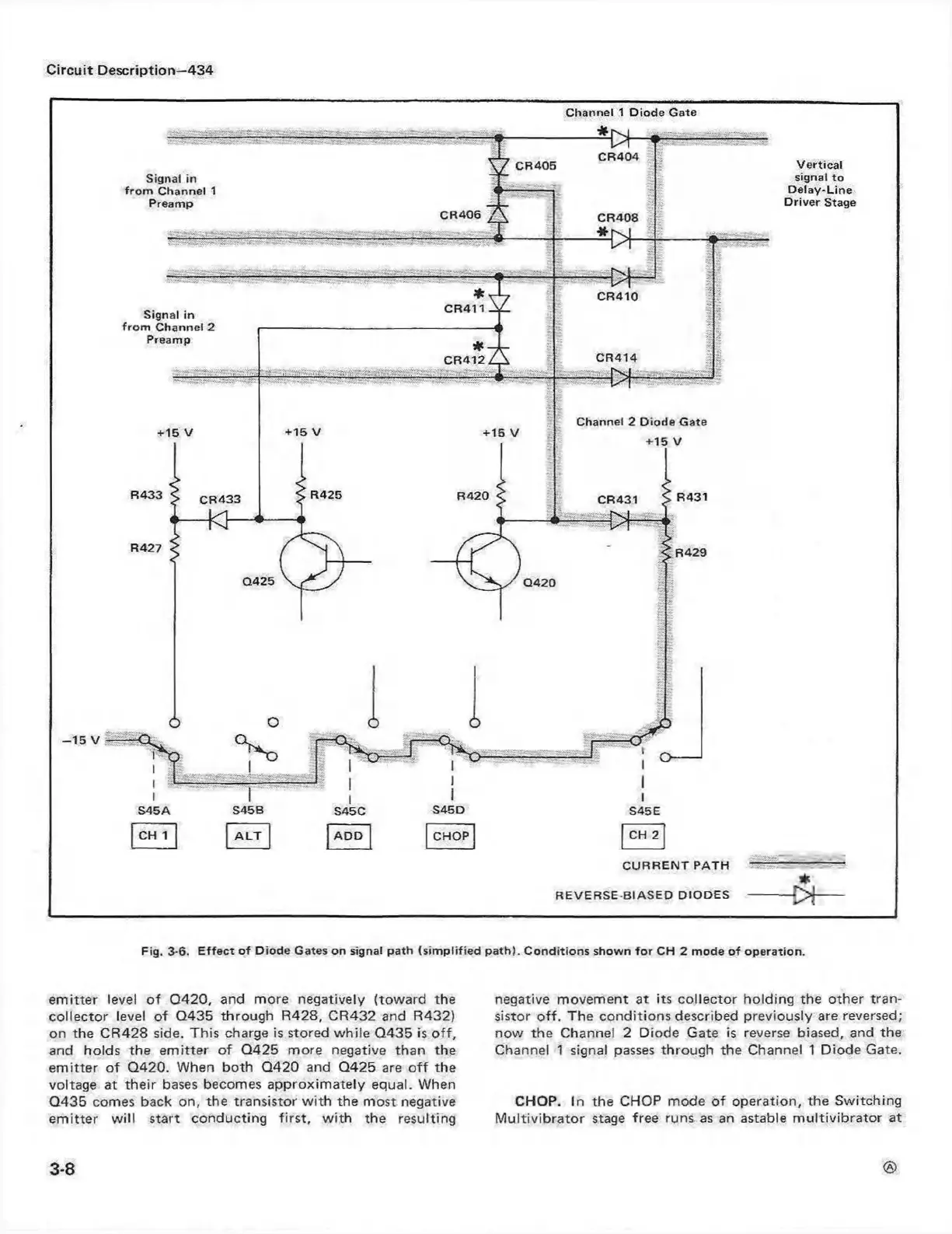
Fig. 3-6. E ffe c t o f D iod e Gates on signal p a th (s im p lifie d p a th ). C o n d itio n s s ho w n fo r CH 2 m ode o f o p e ra tio n .
em itte r level o f Q420, and more negatively (tow ard the
collector level o f Q435 through R428, C R432 and R432)
on the CR 428 side. This charge is stored w hile Q 435 is o ff,
and holds the em itte r o f Q 425 m ore negative than the
em itte r o f Q 420. When both Q 420 and Q425 are o ff the
voltage at the ir bases becomes approxim ately equal. When
Q435 comes back on, the transistor w ith the m ost negative
em itte r w ill start conducting firs t, w ith the resulting
negative m ovem ent at its colle ctor holding the other tra n
sistor o ff. The con dition s described previously are reversed;
now the Channel 2 D iode Gate is reverse biased, and the
Channel 1 signal passes through the Channel 1 Diode Gate.
CHOP. In the CHOP mode o f operation, the Sw itching
M ultiv ib ra to r Stage free runs as an astable m ultiv ib rato r at
3-8