Circuit Description—434
about a 100 kHz rate. The emitters of Q420 and Q425 are
connected to —15 volts through R428, R426, the primary
of T435, and R438. A t the time of turn-on, one of the
transistors begins to conduct; for example, Q420. The
negative level at the collector of Q420 forward biases
CR 405-C R406 and back biases CR404 and CR408,
preventing the Channel 1 signal from reaching the Delay-
Line Driver stage. Meanwhile, the Channel 2 Diode Gate
passes the Channel 2 signal to the Delay-Line Driver stage.
The frequency-determining components in the CHOP
mode are C425-R419-R426-R428. Switching action occurs
as follows: when Q420 is on, C425 attempts to charge to
— 15 volts through R428. The emitter of Q425 slowly goes
toward —15 volts as C425 charges. The base of Q425 is held
at a negative point determined by the voltage divider
R423-R421 between —15 volts and the collector voltage of
Q420. When the em itter voltage of Q425 reaches a level
slightly more negative than its base, Q425 conducts. Its
collector level goes negative and pulls the base of Q420
negative through divider R422-R424 to cut Q420 off. This
switches the Diode Gate stage to connect the opposite half
to the Delay-Line Driver stage. Again C425 begins to charge
toward —15 volts, but this time through R426. The emitter
of Q420 slowly goes negative as C425 charges, until Q420
turns on. Q425 is shut o ff and the cycle begins again.
Diodes CR426 and CR428 are prevented from conducting
by CR432 and R432, so they are effectively removed from
the circuit in the CHOP mode.
The Chopped Blanking A m plifier stage, Q440, provides
an output pulse to the Z Axis A m plifier circuit which
blanks out the transitions between the Channel 1 and the
Channel 2 traces. When the Switching M ultivibrator stage
changes states, the voltage across T435 momentarily
increases. A negative pulse is applied to the base of Q440 to
turn it off. The width of the pulse at the base of Q440 is
determined by R436 and C436. Q440 is quickly driven into
cutoff and the positive-going output pulse, which is
coincident w ith trace switching, is connected to the Z Axis
Am plifier circuit through CR440 and R445.
ADD. In the ADD mode of operation, the Diode Gate
stage allows both signals to pass to the Delay-Line Driver
stage. The Diode Gates are both held on by —15 volts
applied to their cathodes through R450 and R452. Since
both signals are applied to the Delay-Line Driver stage, the
output signal is the algebraic sum of the signals on both
Channels 1 and 2.
Delay-Line Driver
O utput of the Diode Gate stage is applied to the Delay-
Line Driver stage Q454 and Q470. Q454 and Q470 are
connected as feedback amplifiers w ith C456-R456-R457
and C472-R472-R474 providing feedback from the collec
tor to the base of the respective transistor. A sample of the
signal in the collector circuit of Q470 is used for triggering
in the COMP mode of trigger operation. Switch S479
connects capacitor C479 between the output signal lines to
reduce the upper —3 dB bandwidth lim it of the Vertical
A m p lifie r system to a ppro xim ate ly 5 megahertz.
C 4 6 0 -R 4 6 0 and C461-R461 provide high frequency
compensation of the Delay Line term ination. The output of
the Delay-Line Driver stage is connected to the Vertical
O utput A m plifier through the Delay Line.
VER TICAL OUTPUT AMPLIFIER
General
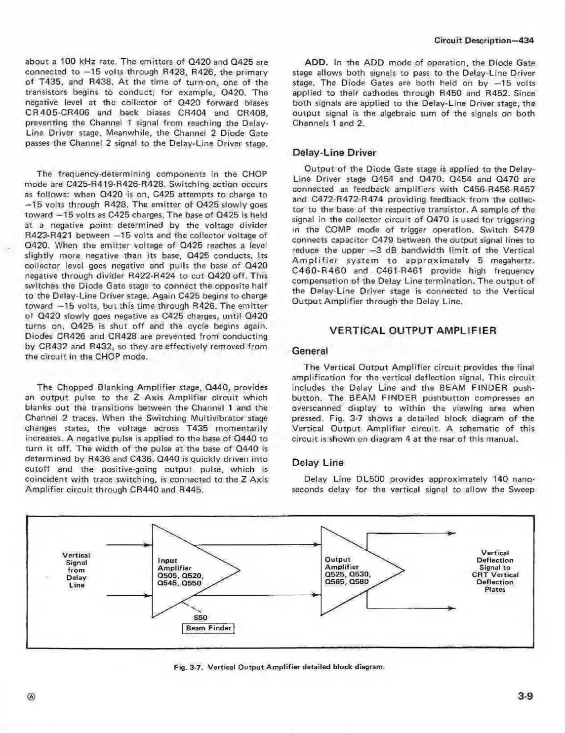
The Vertical O utput A m plifier circuit provides the final
am plification for the vertical deflection signal. This circuit
includes the Delay Line and the BEAM FINDER push
button. The BEAM FINDER pushbutton compresses an
overscanned display to w ith in the viewing area when
pressed. Fig. 3-7 shows a detailed block diagram of the
Vertical O utput A m plifier circuit. A schematic of this
circuit is shown on diagram 4 at the rear of this manual.
Delay Line
Delay Line DL500 provides approximately 140 nano
seconds delay for the vertical signal to allow the Sweep
V ertical
D eflection
Signal to
CRT V e rtica l
D eflection
Plates
3-9
Fig. 3-7. V e rtica l O u tp u t A m p lifie r detailed block diagram.