9 Applications, Implementation, and Layout
9.1 Typical Application
Note
Information in the following applications sections is not part of the TI component specification,
and TI does not warrant its accuracy or completeness. TI’s customers are responsible for
determining suitability of components for their purposes, as well as validating and testing their design
implementation to confirm system functionality.
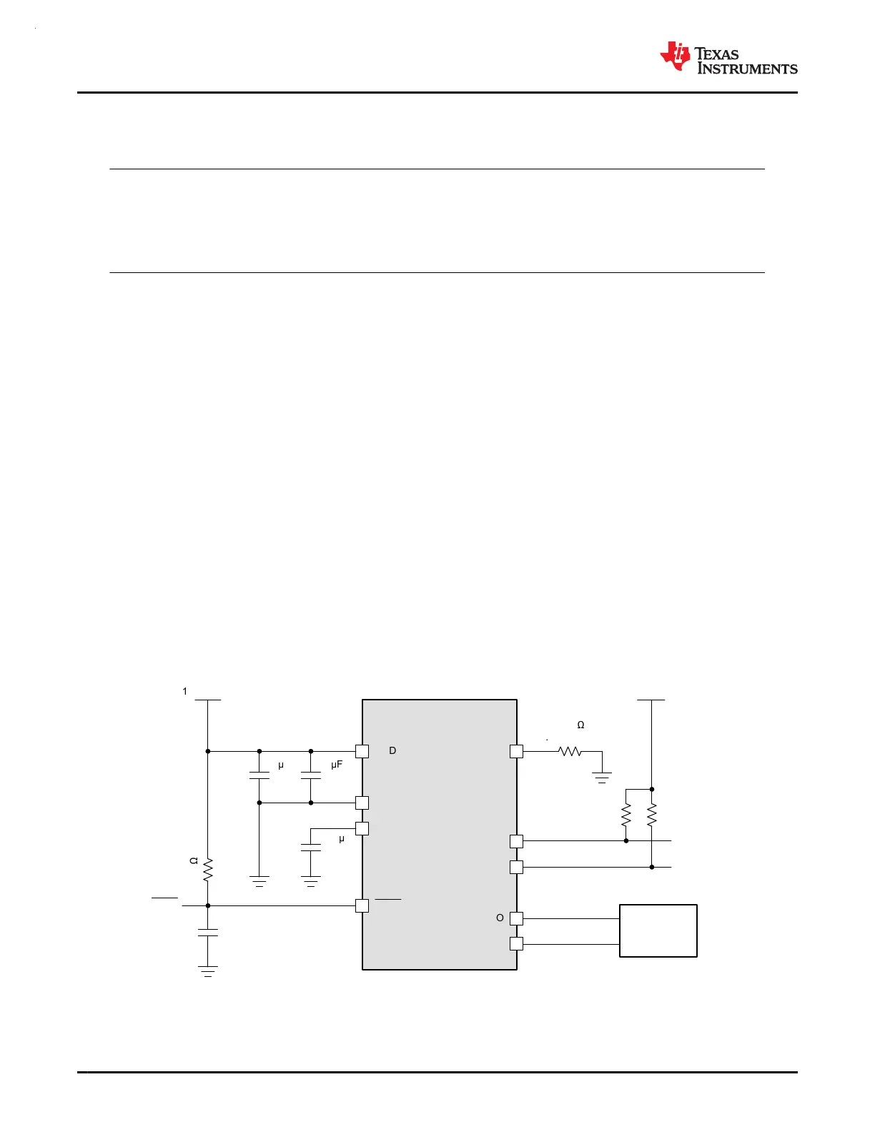
9.1.1 Schematic
TI recommends connecting a combination of a 10-µF and a 0.1-µF low-ESR ceramic decoupling capacitor
across the VDD and VSS pins, as well as placing these capacitors as close as possible to the supply pins that
they decouple (within a few millimeters) to achieve a minimal loop area. The 10-µF bulk decoupling capacitor
is a recommended value for most applications, but this capacitance may be adjusted if needed based upon the
PCB design and application requirements. For example, larger bulk capacitors can be used, but this can affect
the supply rail ramp-up time.
The NRST reset pin must be pulled up to VDD (supply level) for the device to release from RESET state and
start the boot process. TI recommends connecting an external 47-kΩ pullup resistor with a 10-nF pulldown
capacitor for most applications, enabling the NRST pin to be controlled by another device or a debug probe.
The SYSOSC frequency correction loop (FCL) circuit utilizes an external 100-kΩ with 0.1% tolerance resistor
with a temperature coefficient (TCR) of 25ppm/C or better populated between the ROSC pin and VSS. This
resistor establishes a reference current to stabilize the SYSOSC frequency through a correction loop. This
resistor is required if the FCL feature is used for higher accuracy, and it is not required if the SYSOSC FCL is not
enabled. When the FCL mode is not used, the PA2 pin may be used as a digital input/output pin.
A 0.47-µF tank capacitor is required for the VCORE pin and must be placed close to the device with minimum
distance to the device ground. Do not connect other circuits to the VCORE pin.
For the 5-V-tolerant open drain (ODIO), a pullup resistor is required to output high for I2C and UART functions,
as the open drain IO only implement a low-side NMOS driver and no high-side PMOS driver. The 5V-tolerant
open drain IO are fail-safe and may have a voltage present even if VDD is not supplied.
0.1
F10
F
1.62 - 3.6 V
R
OSC
100 k
±0.1% ±25ppm
10nF
NRST
0.47
F
VDD
VSS
VCORE
NRST
MSPM0 MCU
47 k
SWDIO
SWCLK
Debug interface
5V-tolerant open drain pins
Pull-up resistors are required for output high
PA0
PA1
Debug tool
PU
PU
1.62 - 5.5 V
PA2/ROSC
The NRST pullup
resistor and capacitor
are optional, but
NRST must be
pulled high to VDD
for the device to start.
Figure 9-1. Basic Application Schematic
MSPM0G3507, MSPM0G3506, MSPM0G3505
SLASEX6A – FEBRUARY 2023 – REVISED JUNE 2023
www.ti.com
74 Submit Document Feedback
Copyright © 2023 Texas Instruments Incorporated
Product Folder Links: MSPM0G3507 MSPM0G3506 MSPM0G3505
 Loading...


