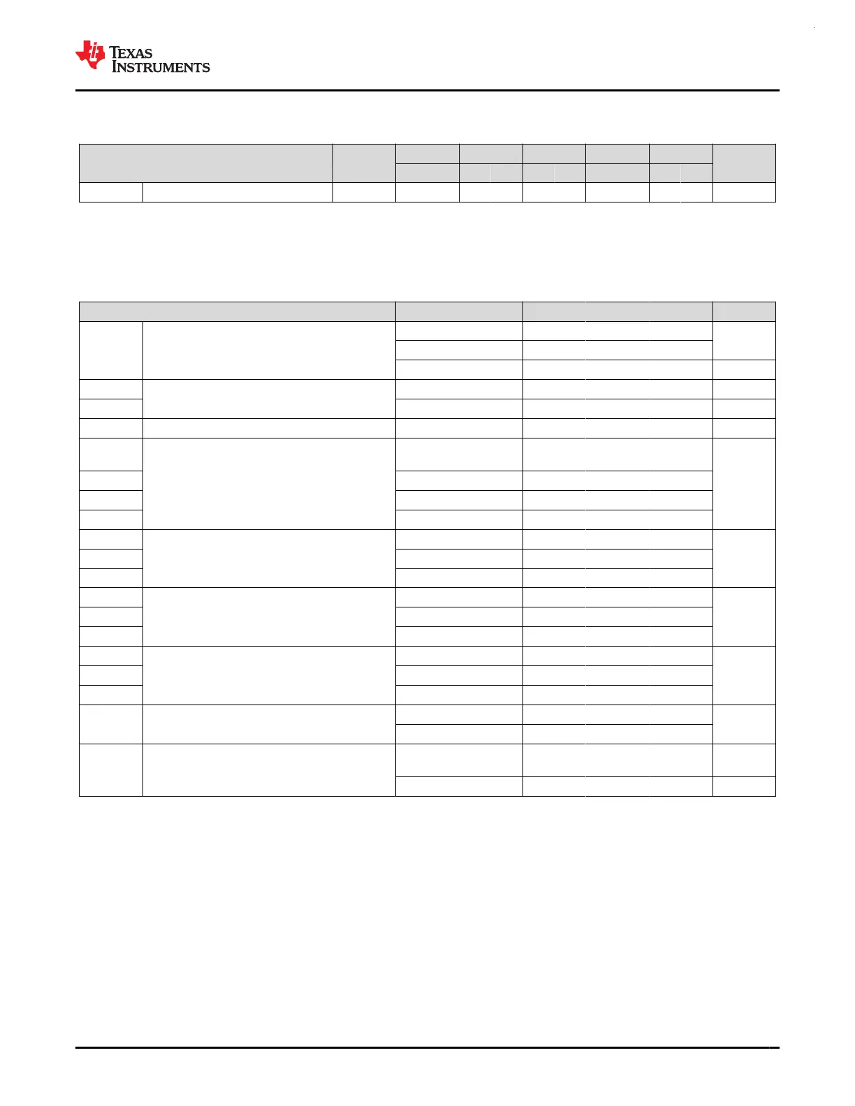
7.5.3 SHUTDOWN Mode
All inputs tied to 0V or VDD. Outputs do not source or sink any current. Core regulator is powered down.
PARAMETER VDD
-40°C 25°C 85°C 105°C 125°C
UNIT
TYP MAX TYP MAX TYP MAX TYP MAX TYP MAX
IDD
SHDN
Supply current in SHUTDOWN mode 3.3V 39 78 676 1625 4688 nA
7.6 Power Supply Sequencing
7.6.1 POR and BOR
over operating free-air temperature range (unless otherwise noted)
PARAMETER TEST CONDITIONS MIN TYP MAX UNIT
dVDD/dt VDD (supply voltage) slew rate
Rising 1
V/us
Falling
(2)
0.01
Falling, STANDBY 0.1 V/ms
V
POR+
Power-on reset voltage level
Rising
(1)
1.04 1.30 1.5 V
V
POR-
Falling
(1)
0.99 1.25 1.48 V
V
HYS, POR
POR hysteresis
(1)
45 58 74 mV
V
BOR0+,
COLD
Brown-out reset voltage level 0 (default level)
Cold start, rising
(1)
1.48 1.54 1.61
V
V
BOR0+
Rising
(1)
(2)
1.58 1.59 1.61
V
BOR0-
Falling
(1)
(2)
1.56 1.57 1.60
V
BOR0, STBY
STANDBY mode
(1)
1.54 1.56 1.60
V
BOR1+
Brown-out-reset voltage level 1
Rising
(1)
(2)
2.15 2.17 2.23
VV
BOR1-
Falling
(1)
(2)
2.12 2.14 2.19
V
BOR1, STBY
STANDBY mode
(1)
2.06 2.13 2.20
V
BOR2+
Brown-out-reset voltage level 2
Rising
(1)
(2)
2.74 2.77 2.83
VV
BOR2-
Falling
(1)
(2)
2.71 2.73 2.80
V
BOR2, STBY
STANDBY mode
(1)
2.68 2.71 2.82
V
BOR3+
Brown-out-reset voltage level 3
Rising
(1)
(2)
2.88 2.96 3.04
VV
BOR3-
Falling
(1)
(2)
2.85 2.93 3.01
V
BOR3, STBY
STANDBY mode
(1)
2.80 2.92 3.02
V
HYS,BOR
Brown-out reset hysteresis
Level 0
(1)
14 18
mV
Levels 1-3
(1)
34 38
T
PD, BOR
BOR propagation delay
RUN/SLEEP/STOP
mode
10 us
STANDBY mode 100 us
(1) |dVDD/dt| ≤ 3V/s
(2) Device operating in RUN, SLEEP, or STOP mode.
7.6.2 Power Supply Ramp
Figure 7-1 gives the relationship of POR- POR+, BOR0-, and BOR0+ during power-up and power-down.
www.ti.com
MSPM0G3507, MSPM0G3506, MSPM0G3505
SLASEX6A – FEBRUARY 2023 – REVISED JUNE 2023
Copyright © 2023 Texas Instruments Incorporated
Submit Document Feedback
31
Product Folder Links: MSPM0G3507 MSPM0G3506 MSPM0G3505
 Loading...


