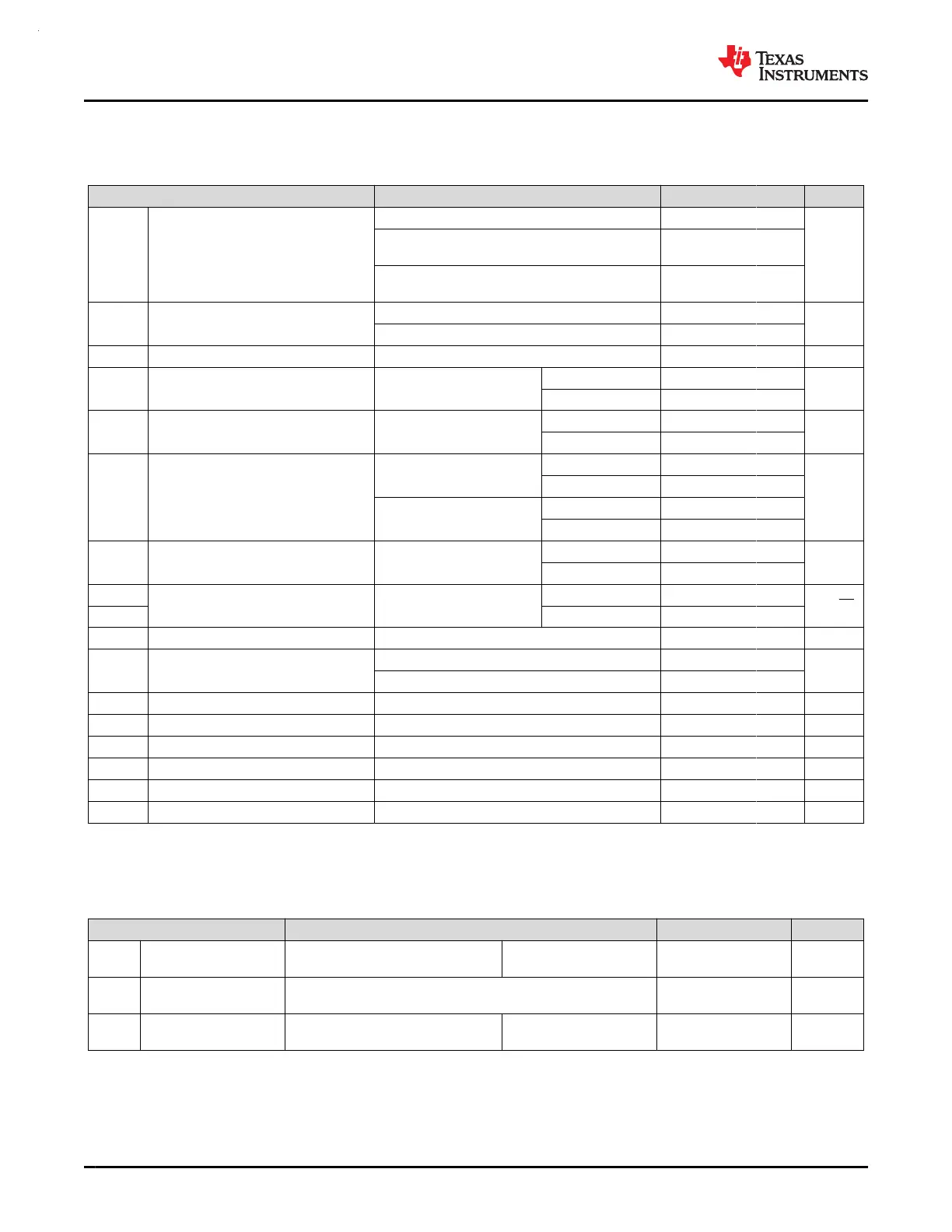
7.17 GPAMP
7.17.1 Electrical Characteristics
over recommended ranges of supply voltage and operating free-air temperature (unless otherwise noted)
PARAMETER TEST CONDITIONS MIN TYP MAX UNIT
V
CM
Common mode voltage range
RRI = 0x0 -0.1 VDD–1
V
RRI = 0x1 1
VDD-0.
2
RRI = 0x2 -0.1
VDD-0.
2
I
q
Quiescent current, per op-amp
I
O
= 0 mA, RRI = 0x0 97
µA
I
O
= 0 mA, RRI = 0x1 or 0x2 93
GBW Gain-bandwidth product C
L
= 200pF 0.32 MHz
V
OS
Input offset voltage
Noninverting, unity gain, T
A
= 25℃, VDD = 3.3V
CHOP = 0x0 ±0.2 ±6.5
mV
CHOP = 0x1 ±0.08 ±0.4
dV
OS
/dT Input offset voltage temperature drift Noninverting, unity gain
CHOP = 0x0 7.7
µV/°C
CHOP = 0x1 0.34
I
bias
Input bias for muxed I/O pin at SoC
0.1V<V
in
<VDD-0.3V,
VDD=3.3V, CHOP=0x0
T
A
= 25°C ±40
pA
T
A
= 125°C ±4000
0.1V<V
in
<VDD-0.3V,
VDD=3.3V, CHOP = 0x1
T
A
= 25°C ±200
T
A
= 125°C ±4000
CMRR
DC
Common mode rejection ratio, DC
Over common mode voltage
range
CHOP = 0x0 48 77
dB
CHOP = 0x1 56 105
e
n
Input voltage noise density Noninverting, unity gain
f = 1 kHz 43
nV/√Hz
e
n
f = 10 kHz 19
R
in
Input resistance
(1)
0.65 kΩ
C
in
Input capacitance
Common mode 4
pF
Differential 2
A
OL
Open-loop voltage gain, DC R
L
= 350 kΩ, 0.3 < Vo < VDD-0.3 82 90 107 dB
PM phase margin C
L
= 200 pF, R
L
= 350 kΩ 69 70 72 degree
SR Slew rate Noninverting, unity gain, C
L
= 40 pF 0.32 V/µs
THDN Total Harmonic Distortion + Noise 0.012 %
I
Load
Output load current ±10 µA
C
Load
Output load capacitance 200 pF
(1) R
in
here means the input resistance of mux in GPAMP.
7.17.2 Switching Characteristics
over recommended ranges of supply voltage and operating free-air temperature (unless otherwise noted)
PARAMETER TEST CONDITIONS MIN TYP MAX UNIT
t
EN
GPAMP enable time
ENABLE = 0x0 to 0x1, Bandgap
reference ON, 0.1%
Noninverting, unity gain 12 20 µs
t
disable
GPAMP disable time 4
ULPCLK
Cycles
t
SETTLE
GPAMP settling time
C
L
= 200 pF, Vstep = 0.3V to VDD -
0.3V, 0.1%, ENABLE = 0x1
Noninverting, unity gain 9 µs
MSPM0G3507, MSPM0G3506, MSPM0G3505
SLASEX6A – FEBRUARY 2023 – REVISED JUNE 2023
www.ti.com
44 Submit Document Feedback
Copyright © 2023 Texas Instruments Incorporated
Product Folder Links: MSPM0G3507 MSPM0G3506 MSPM0G3505
 Loading...


