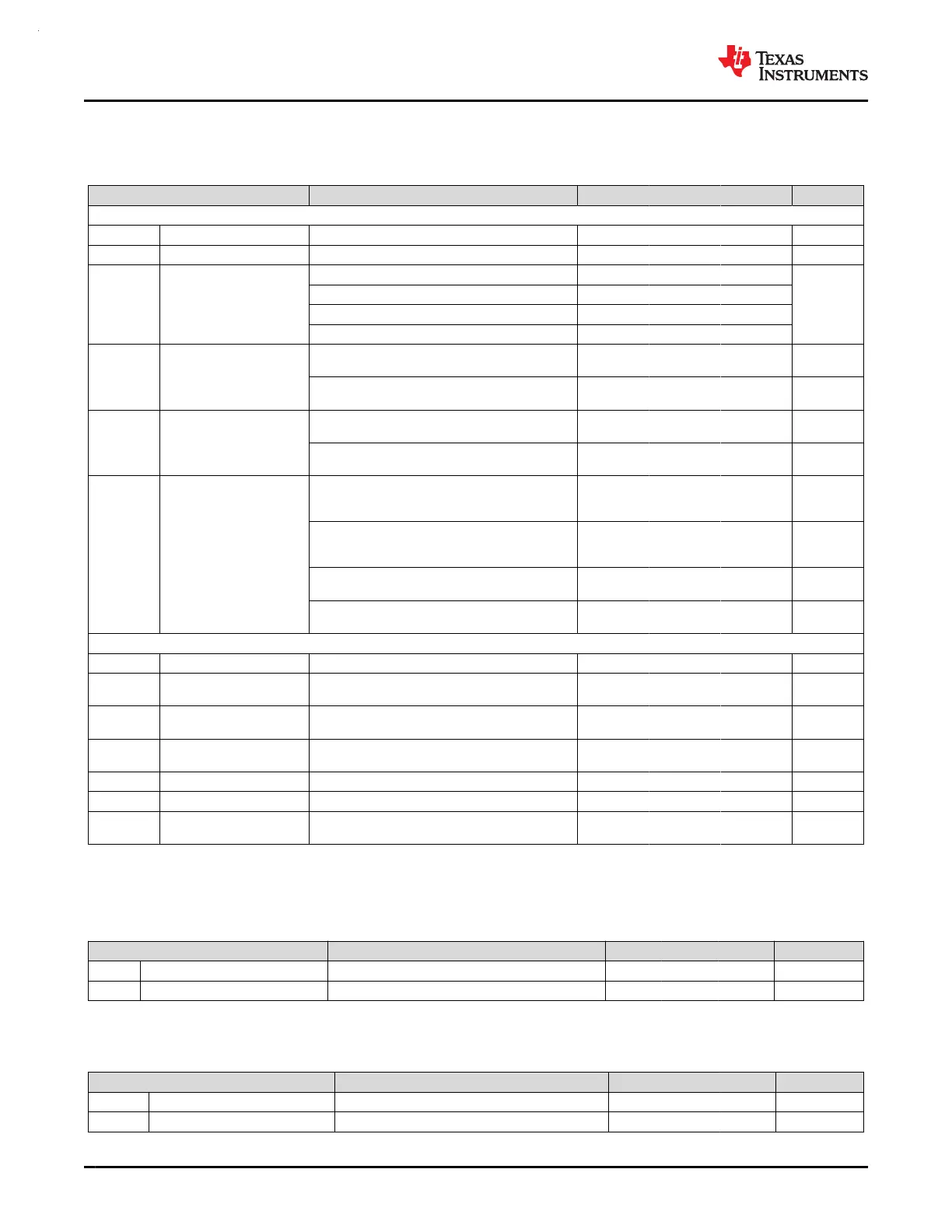
7.15 Comparator (COMP)
7.15.1 Comparator Electrical Characteristics
over recommended ranges of supply voltage and operating free-air temperature (unless otherwise noted)
PARAMETER TEST CONDITIONS MIN TYP MAX UNIT
Comparator Electrical Characteristics
Vcm Common mode input range 0 VDD V
V
offset
Input offset voltage ±25 mV
V
hys
DC input hysteresis
HYST=00h 0.4
mV
HYST=01h 11
HYST=02h 20
HYST=03h 30
t
PD_ls
Propagation delay, response
time
Output Filter off, Overdrive = 100 mV, High Speed
Mode
32 50 ns
Output Filter off, Overdrive = 100 mV, Low Power
Mode
5 µs
t
en
Comparator enable time
Startup time to reach propagation delay
specification, High Speed Mode (comparator only)
10 µs
Startup time to reach propagation delay
specification, Low Power Mode (comparator only)
10 µs
I
comp
Comparator current
consumption.
Vcm = VDD/2, 100mV overdrive, DAC output as a
voltage reference, VDD is reference for DAC, High
Speed Mode
120 200 µA
Vcm = VDD/2, 100mV overdrive, DAC output as a
voltage reference, VDD is reference for DAC, Low
Power Mode
0.8 2.7 µA
Vcm = VDD/2, 100mV overdrive, comparator only.
High Speed Mode
100 180 µA
Vcm = VDD/2, 100mV overdrive, comparator
only, Low Power Mode
0.7 2.1 µA
8-bit DAC Electrical Characteristics
V
dac
DAC output range 0 VDD V
V
dac-code
8-bit DAC output voltage for
a given code
VIN = reference voltage into 8-bit DAC, code n = 0 to
255
VIN ×
(n+1) / 256
V
INL
Integral nonlinearity of 8-bit
DAC
-1 1 LSB
DNL
Differential nonlinearity of 8-
bit DAC
-1 1 LSB
Gain error Gain error of 8-bit DAC Reference voltage = VDD -2 2 % of FSR
Offset error Offset error of 8-bit DAC -5 5 mV
t
dac_settle
8-bit DAC settling time in
static mode
DACCODE0 = 0 → 255, DAC output accurate to 1
LSB
1.5 µs
7.16 DAC
7.16.1 DAC_Supply Specifications
over recommended ranges of supply voltage and operating free-air temperature (unless otherwise noted)
PARAMETER TEST CONDITIONS MIN TYP MAX UNIT
V
REF
Reference voltage VDD, External, Internal(1.4V, 2.5V) 1.4 VDD V
I
DAC
DAC current consumption from VDD VREF= VDD, No load 300 µA
7.16.2 DAC Output Specifications
over recommended ranges of supply voltage and operating free-air temperature (unless otherwise noted)
PARAMETER TEST CONDITIONS MIN TYP MAX UNIT
V
O
Output voltage range No load, Vref = VDD, DATA = 0x0 0 0.005 0.05 V
V
O
Output voltage range No load, Vref = VDD, DATA = 0xFFF VDD-0.05 -0.01 VDD V
MSPM0G3507, MSPM0G3506, MSPM0G3505
SLASEX6A – FEBRUARY 2023 – REVISED JUNE 2023
www.ti.com
42 Submit Document Feedback
Copyright © 2023 Texas Instruments Incorporated
Product Folder Links: MSPM0G3507 MSPM0G3506 MSPM0G3505
 Loading...


