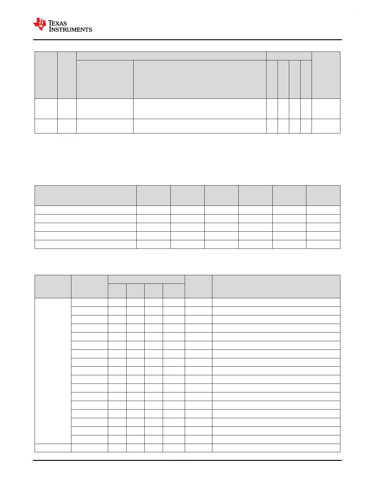
Table 6-1. Pin Attributes (continued)
PINCMx
PIN
NAME
SIGNAL NAMES PIN NUMBER
IO
STRUCTU
RE
ANALOG DIGITAL [PIN FUNCTION]
(1)
64 LQFP
48 LQFP, VQFN
32 VQFN
28 VSSOP
59
PA26 A0_1 / COMP0_IN0+ /
OPA0_IN0+ /
GPAMP_IN+
UART3_TX [2] / SPI1_CS0 [3] / TIMG8_C0 [4] /
TIMA_FAL0 [5] / CAN_TX [6] / TIMG7_C0 [7]
30 46 30 1 Standard
60
PA27 A0_0 / COMP0_IN0- /
OPA0_IN0-
RTC_OUT [2] / SPI1_CS1 [3] / TIMG8_C1 [4] / TIMA_FAL2
[5] / CAN_RX [6] / TIMG7_C1 [7]
31 47 31 2 Standard
(1) PINCM.PF and PINCM.PC in IOMUX should be set to 0 for analog functions (i.e. OPA inputs/outputs, COMP inputs, etc.). Each digital
I/O on a device is mapped to a specific Pin Control Management Register (PINCMx) which allows users to configure the desired Pin
Function using the PINCM.PF control bits.
(2) Standard with Wake allows the I/O to wake up the device from the lowest low-power mode of SHUTDOWN. All I/O can be configured
to wakeup the MCU from higher low-power modes. See section GPIO FastWake in the MSPM0 G-Series 80-MHz Microcontrollers
Technical Reference Manual for details.
Table 6-2. Digital IO Features by IO Type
IO STRUCTURE
INVERSION
CONTROL
DRIVE
STRENGTH
CONTROL
HYSTERESIS
CONTROL
PULLUP
RESISTOR
PULLDOWN
RESISTOR
WAKEUP
LOGIC
Standard drive Y Y Y
Standard drive with wake
(2)
Y Y Y Y
High drive Y Y Y Y Y
High speed Y Y Y Y
5-V tolerant open drain Y Y Y Y
6.3 Signal Descriptions
Table 6-3. Signal Descriptions
FUNCTION
SIGNAL
NAME
PIN NO.
(1)
PIN TYPE
(2)
DESCRIPTION
64 PM
48 PT,
RGZ
32
RHB
28
DGS28
ADC
A0_0 31 47 31 2 I ADC0 analog input 0
A0_1 30 46 30 1 I ADC0 analog input 1
A0_2 26 45 29 28 I ADC0 analog input 2
A0_3 25 44 28 27 I ADC0 analog input 3
A0_4 27 – – – I ADC0 analog input 4
A0_5 23 42 – – I ADC0 analog input 5
A0_6 19 41 – – I ADC0 analog input 6
A0_7 18 40 26 25 I ADC0 analog input 7
A0_12 7 29 18 17 I ADC0 analog input 12
A1_0 8 30 19 18 I ADC1 analog input 0
A1_1 9 31 20 19 I ADC1 analog input 1
A1_2 10 32 21 20 I ADC1 analog input 2
A1_3 11 33 22 21 I ADC1 analog input 3
A1_4 14 36 – – I ADC1 analog input 4
A1_5 15 37 – – I ADC1 analog input 5
A1_6 16 38 – – I ADC1 analog input 6
A1_7 17 39 25 24 I ADC1 analog input 7
BSL BSL_invoke 11 33 22 21 I Input pin used to invoke bootloader
www.ti.com
MSPM0G3507, MSPM0G3506, MSPM0G3505
SLASEX6A – FEBRUARY 2023 – REVISED JUNE 2023
Copyright © 2023 Texas Instruments Incorporated
Submit Document Feedback
15
Product Folder Links: MSPM0G3507 MSPM0G3506 MSPM0G3505
 Loading...


