8.30 Device Analog Connections
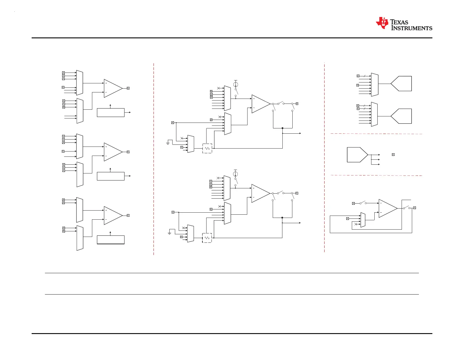
Figure 8-1 shows the internal analog connection of the device.
OPA0
OPA0_IN1-
OPA0_OUT
2
3
4
OPA0_IN0+
OPA0_IN0-
0
1
2
RTOPRBOT
RTAP
3
0
1
DAC_OUT / OPA0_IN2+
VDDA
Burnout
current
source
0
2
3
4
1
5
Internal signal
to ADC0 and
COMP0
DAC_OUT / OPA0_IN2+
DAC8.0_OUT
OPA1_RBOT
VREF+
5
OPA1
OPA1_IN1-
OPA1_OUT
OPA1_IN0-
RTOPRBOT
RTAP
VDDA
Burnout
current
source
Internal signal
to ADC1 and
COMP0
OPA0_RBOT
ADC0
8
11
12
0:7
13
0
2
3
4
1
5
14
A0_0:A0_7
A1_7
Temp Sense
A0_12
OPA0 Output
GPAMP Output
GPAMP
GPAMP_IN+
GPAMP_IN-
0
2
3
1
Internal signal to
ADC0, ADC1,
OPA0, and OPA1
GPAMP_OUT
15
Supply/Battery Monitor
ADC1
8
12
1:7
13
14
A1_1:A1_7
A0_7
Temp Sense
OPA1 Output
GPAMP Output
15
Supply/Battery Monitor
6
OPA1_RTOP
GPAMP_OUT
7
OPA0_IN1+
2
3
4
OPA1_IN0+
0
1
DAC_OUT / OPA1_IN2+
DAC8.1_OUT
VREF+
5
6
OPA0_RTOP
GPAMP_OUT
7
OPA1_IN1+
4
OPA1_RTOP
0
1
2
3
4
DAC_OUT / OPA1_IN2+
OPA0_RTOP
COMP
0
COMP0_OUT
2
0
1
0
2
5
1
6
DAC_OUT / COMP0_IN3+ 5
6
OPA1_OUT
COMP1 positive terminal
7
Reference Generator
8-bit DAC8.0
OPA0+
COMP0 Ref
COMP0_IN0+
COMP0_IN1+
COMP0_IN2+
Temp sensor output
OPA0_OUT
COMP0_IN0-
COMP0_IN1-
COMP0_IN2-
COMP
1
COMP1_OUT
2
0
1
0
2
1
DAC_OUT /
COMP1_IN3+
5
COMP0 positive terminal
7
Reference Generator
8-bit DAC8.1
OPA1+
COMP1 Ref
COMP1_IN0+
COMP1_IN1+
COMP1_IN2+
COMP1_IN0-
COMP1_IN1-
COMP1_IN2-
COMP
2
COMP2_OUT
0
1
0
1
Reference Generator
8-bit DAC8.2
COMP2 Ref
COMP0_IN0+
COMP0_IN1+
COMP0_IN0-
COMP0_IN1-
Comparators Op-amps
ADC
GPAMP
DAC
12bit
Buffered
DAC
DAC_OUT
COMP0+
COMP1+
0
A1_0 / DAC_OUT
Figure 8-1. Device Analog Connection
Note
Enabling DAC_OUT connects to PA15 therefore it is not recommended to have any external signal on PA15 when using DAC_OUT.
MSPM0G3507, MSPM0G3506, MSPM0G3505
SLASEX6A – FEBRUARY 2023 – REVISED JUNE 2023
www.ti.com
70 Submit Document Feedback
Copyright © 2023 Texas Instruments Incorporated
Product Folder Links: MSPM0G3507 MSPM0G3506 MSPM0G3505
 Loading...


