– External reference supplied to the ADC through the VREF+/- pins
• Operates in RUN, SLEEP, and STOP modes
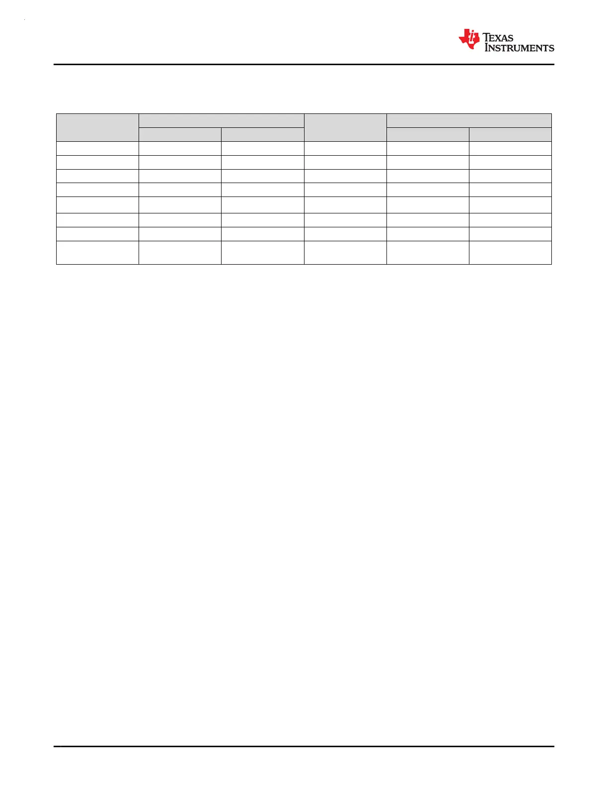
Table 8-7. ADC Channel Mapping
CHANNEL[0:7]
SIGNAL NAME
(2)
CHANNEL[8:15]
SIGNAL NAME
(1)
(2)
ADC0 ADC1 ADC0 ADC1
0 A0_0 A1_0 / DAC_OUT
(4)
8 A1_7
(3)
A0_7
(3)
1 A0_1 A1_1 9 - -
2 A0_2 A1_2 10 - -
3 A0_3 A1_3 11 Temperature Sensor -
4 A0_4 A1_4 12 A0_12 Temperature Sensor
5 A0_5 A1_5 13 OPA0 output OPA1 output
6 A0_6 A1_6 14 GPAMP output GPAMP output
7 A0_7 A1_7 15
Supply/Battery
Monitor
Supply/Battery
Monitor
(1) Italicized signal names are purely internal to the SoC. These signals are used for internal peripheral interconnections.
(2) For more information about device analog connections please refer to Section 8.30
(3) Note that each channel 8 of each ADC can be sampled by the opposite ADC.
(4) When DAC_OUT is used, A1_0 cannot be used to sample external signals. Avoid using external circuitry on the PA15 pin when using
DAC_OUT.
For more details, see the ADC chapter of the MSPM0 G-Series 80-MHz Microcontrollers Technical Reference
Manual.
8.13 Temperature Sensor
The temperature sensor provides a voltage output that changes linearly with device temperature. The
temperature sensor output is internally connected to one of ADC input channels to enable a temperature-to-
digital conversion.
A unit-specific single-point calibration value for the temperature sensor is provided in the factory constants
memory region. This calibration value represents the ADC conversion result (in ADC code format) corresponding
to the temperature sensor being measured in 12-bit mode with the 1.4-V internal VREF at the factory trim
temperature (TS
TRIM
). The ADC and VREF configuration for the above measurement is as the following: RES=0
(12-bit mode), VRSEL=2h (internal VREF), BUFCONFIG=1h (1.4V VREF), ADC t
Sample
=12.5µs. This calibration
value can be used with the temperature sensor temperature coefficient (TS
c
) to estimate the device temperature.
See the temperature sensor section of the MSPM0 G-Series 80-MHz Microcontrollers Technical Reference
Manual for guidance on estimating the device temperature with the factory trim value.
8.14 VREF
The shared voltage reference module (VREF) in these devices contain a configurable voltage reference buffer
which allows users to supply a stable reference to on-board analog peripherals. It also supports bringing in an
external reference for applications where higher accuracy is required.
VREF features include:
• 1.4V and 2.5V user-selectable internal references
• Internal reference supports full speed ADC operation
• Support for bringing in an external reference on VREF+/- device pins
• Requires a decoupling capacitor placed on VREF+/- pins for proper operation. See VREF specification
section for more details
For more details, see the VREF chapter of the MSPM0 G-Series 80-MHz Microcontrollers Technical Reference
Manual.
8.15 COMP
The comparator peripheral in the device compares the voltage levels on two inputs terminals and provides a
digital output based on this comparison. It supports the following key features:
MSPM0G3507, MSPM0G3506, MSPM0G3505
SLASEX6A – FEBRUARY 2023 – REVISED JUNE 2023
www.ti.com
62 Submit Document Feedback
Copyright © 2023 Texas Instruments Incorporated
Product Folder Links: MSPM0G3507 MSPM0G3506 MSPM0G3505
 Loading...


