3. T (Min sampling time) = K*Tau
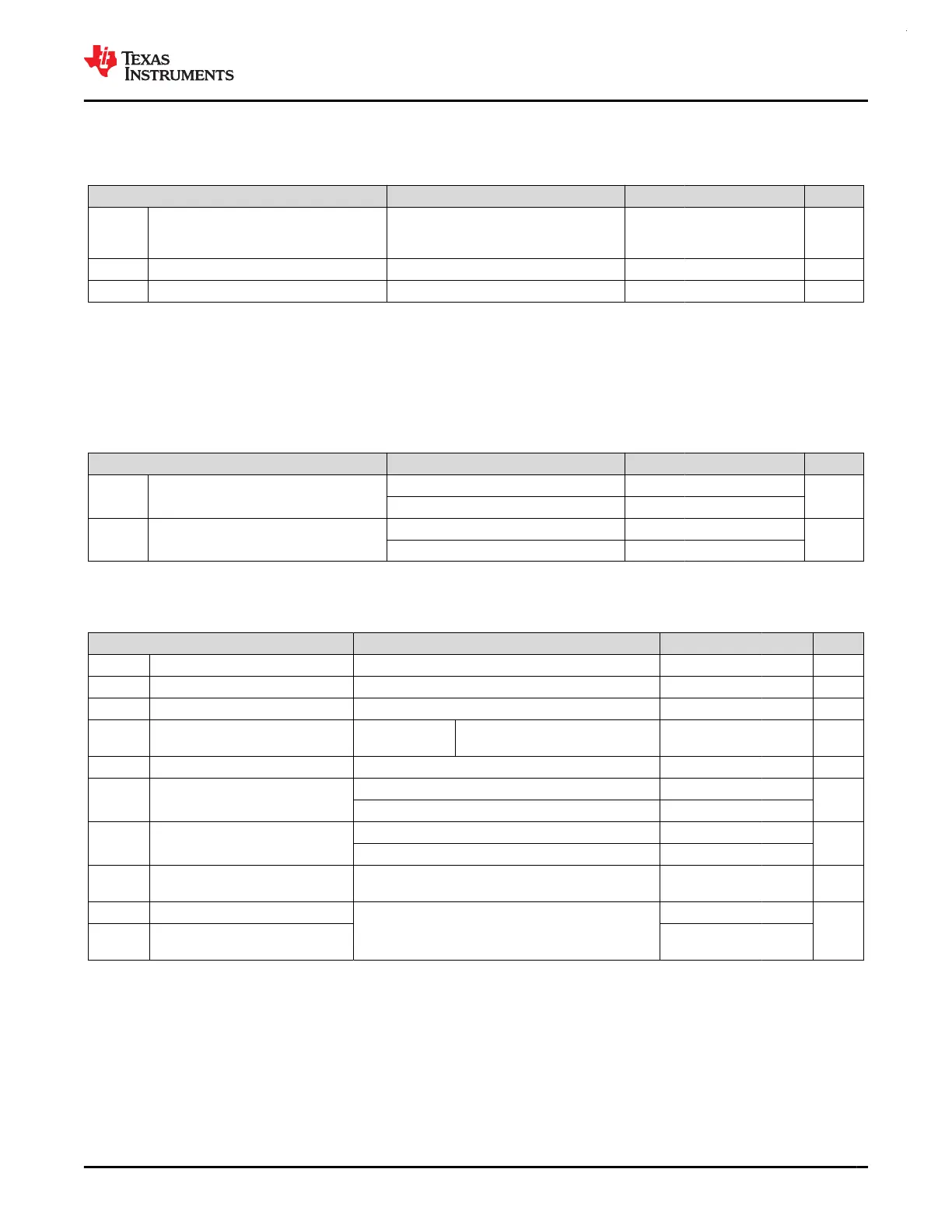
7.13 Temperature Sensor
over operating free-air temperature range (unless otherwise noted)
PARAMETER TEST CONDITIONS MIN TYP MAX UNIT
TS
TRIM
Factory trim temperature
(1)
ADC and VREF configuration: RES=0
(12-bit mode), VRSEL=0h (VDDA=3.3V),
ADC t
Sample
=12.5µs
27 30 33 ℃
TS
c
Temperature coefficient -40℃ ≤ T
j
≤ 130℃ -1.84 -1.75 -1.66 mV/℃
t
SET, TS
Temperature sensor settling time
(2)
2.5 10 us
(1) Higher absolute accuracy may be achieved through user calibration. Please refer to temperature sensor chapter in detailed description
section.
(2) This is the minimum required ADC sampling time when measuring the temperature sensor.
7.14 VREF
7.14.1 Voltage Characterisitcs
over recommended ranges of supply voltage and operating free-air temperature (unless otherwise noted)
PARAMETER TEST CONDITIONS MIN TYP MAX UNIT
VDD
min
Minimum supply voltage needed for
VREF operation
BUFCONFIG = 0 2.7
V
BUFCONFIG = 1 1.62
VREF Voltage reference output voltage
BUFCONFIG = 1 1.379 1.4 1.421
V
BUFCONFIG = 0 2.462 2.5 2.538
7.14.2 Electrical Characteristics
over recommended ranges of supply voltage and operating free-air temperature (unless otherwise noted)
PARAMETER TEST CONDITIONS MIN TYP MAX UNIT
I
VREF
VREF operating supply current BUFCONFIG = {0, 1}, No load 200 350 µA
I
Drive
VREF output drive strength
(1)
Drive strength supported on VREF+ device pin 100 µA
I
SC
VREF short circuit current 100 mA
TC
VREF
Temperature coefficient of VREF
(Bandgap+VRBUF)
(3)
BUFCONFIG =
{0, 1}
BUFCONFIG = {0, 1} 200 ppm/°C
TC
drift
Long term VREF drift Time = 1000 hours, BUFCONFIG = {0, 1}, T = 25℃ 300 ppm
PSRR
DC
VREF Power supply rejection ratio,
DC
VDD = 1.7 V to VDDmax, BUFCONFIG = 1 -59 -62
dB
VDD = 2.7 V to VDDmax, BUFCONFIG = 0 -49 -52
V
noise
RMS noise at VREF output (0.1 Hz
to 100 MHz)
BUFCONFIG = 1 500
µVrms
BUFCONFIG = 0 900
C
VREF
Recommended VREF decoupling
capacitor on VREF+ pin
(3)
(4)
(5)
0.7 1 1.15 µF
T
startup
VREF startup time
BUFCONFIG = {0, 1} , VDD = 2.8 V, C
VREF
= 1µF
200
µS
T
refresh
VREF External capacitor refresh
time
31.25
(1) The specified MAX output drive strength is supported regardless of which peripherals are being used in the device.
(2) The temperature coefficient of the VREF output is the sum of TC
VRBUF
and the temperature coefficient of the internal bandgap
reference.
(3) Decoupling capacitor (C
VREF
) is required when using the internal voltage reference VREF and should be connected from the VREF+
pin to VREF-/GND. When using the VREF+/- pins to supply an external reference, a decoupling capacitor value should be selected
based on the external reference source.
(4) A ceramic capacitor with package size of 0805 or smaller is preferred. Up to ±20% tolerance is acceptable
(5) The VREF module should only be enabled when C
VREF
is connected and should not be enabled otherwise.
www.ti.com
MSPM0G3507, MSPM0G3506, MSPM0G3505
SLASEX6A – FEBRUARY 2023 – REVISED JUNE 2023
Copyright © 2023 Texas Instruments Incorporated
Submit Document Feedback
41
Product Folder Links: MSPM0G3507 MSPM0G3506 MSPM0G3505
 Loading...


