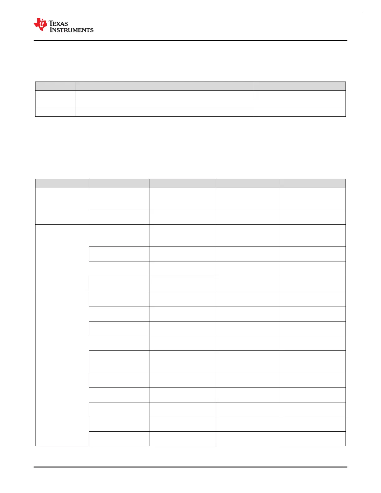
Table 8-3. Generic Event Channels (continued)
A generic route is either a point-to-point (1:1) route or a point-to-two (1:2) splitter route route in which the peripheral
publishing the event is configured to use one of several available generic route channels to publish its event to another entity
(or entities, in the case of a splitter route), where an entity may be another peripheral, a generic DMA trigger event, or a
generic CPU event.
CHANID Generic Route Channel Selection Channel Type
13 Generic event channel 13 selected 1 : 2 (splitter)
14 Generic event channel 14 selected 1 : 2 (splitter)
15 Generic event channel 15 selected 1 : 2 (splitter)
8.7 Memory
8.7.1 Memory Organization
Table 8-4 summarizes the memory map of the devices. For more information about the memory region detail,
see the Platform Memory Map section in the MSPM0 G-Series 80-MHz Microcontrollers Technical Reference
Manual .
Table 8-4. Memory Organization
MEMORY REGION SUBREGION MSPM0G3505 MSPM0G3506 MSPM0G3507
Code (Flash)
MAIN ECC Corrected
32KB-8B
(1)
0x0000.0000 to
0x0000.7FF8
64KB-8B
(1)
0x0000.0000 to
0x0000.FFF8
128KB-8B
(1)
0x0000.0000 to
0x0001.FFF8
MAIN ECC Uncorrected
0x0040.0000 to
0x0040.7FF8
0x0040.0000 to
0x0040.FFF8
0x0040.0000 to
0x0041.FFF8
SRAM (SRAM)
Default (ECC Corrected)
(2)
16KB
0x2000.0000 to
0x200F.FFFF
32KB
0x2000.0000 to
0x200F.FFFF
32KB
0x2000.0000 to
0x200F.FFFF
Parity checked
0x2010.0000 to
0x201F.FFFF
0x2010.0000 to
0x201F.FFFF
0x2010.0000 to
0x201F.FFFF
Un-checked
0x2020.0000 to
0x202F.FFFF
0x2020.0000 to
0x202F.FFFF
0x2020.0000 to
0x202F.FFFF
ECC/parity
code
0x2030.0000 to
0x203F.FFFF
0x2030.0000 to
0x203F.FFFF
0x2030.0000 to
0x203F.FFFF
Peripheral
Peripherals
0x4000.0000 to
0x40FF.FFFF
0x4000.0000 to
0x40FF.FFFF
0x4000.0000 to
0x40FF.FFFF
MAIN Corrected
0x4100.0000 to
0x4100.8000
0x4100.0000 to
0x4101.0000
0x4100.0000 to
0x4102.0000
MAIN Uncorrected
0x4140.0000 to
0x4140.8000
0x4140.0000 to
0x4141.0000
0x4140.0000 to
0x4142.0000
MAIN ECC code
0x4180.0000 to
0x4180.8000
0x4180.0000 to
0x4181.0000
0x4180.0000 to
0x4182.0000
NONMAIN Corrected
512 bytes
0x41C0.0000 to
0x41C0.0200
512 bytes
0x41C0.0000 to
0x41C0.0200
512 bytes
0x41C0.0000 to
0x41C0.0200
NONMAIN Uncorrected
0x41C1.0000 to
0x41C1.0200
0x41C1.0000 to
0x41C1.0200
0x41C1.0000 to
0x41C1.0200
NONMAIN ECC code
0x41C2.0000 to
0x41C2.0200
0x41C2.0000 to
0x41C2.0200
0x41C2.0000 to
0x41C2.0200
FACTORY Corrected
0x41C4.0000 to
0x41C4.0080
0x41C4.0000 to
0x41C4.0080
0x41C4.0000 to
0x41C4.0080
FACTORY Uncorrected
0x41C5.0000 to
0x41C5.0080
0x41C5.0000 to
0x41C5.0080
0x41C5.0000 to
0x41C5.0080
FACTORY ECC code
0x41C6.0000 to
0x41C6.0080
0x41C6.0000 to
0x41C6.0080
0x41C6.0000 to
0x41C6.0080
www.ti.com
MSPM0G3507, MSPM0G3506, MSPM0G3505
SLASEX6A – FEBRUARY 2023 – REVISED JUNE 2023
Copyright © 2023 Texas Instruments Incorporated
Submit Document Feedback
57
Product Folder Links: MSPM0G3507 MSPM0G3506 MSPM0G3505
 Loading...


