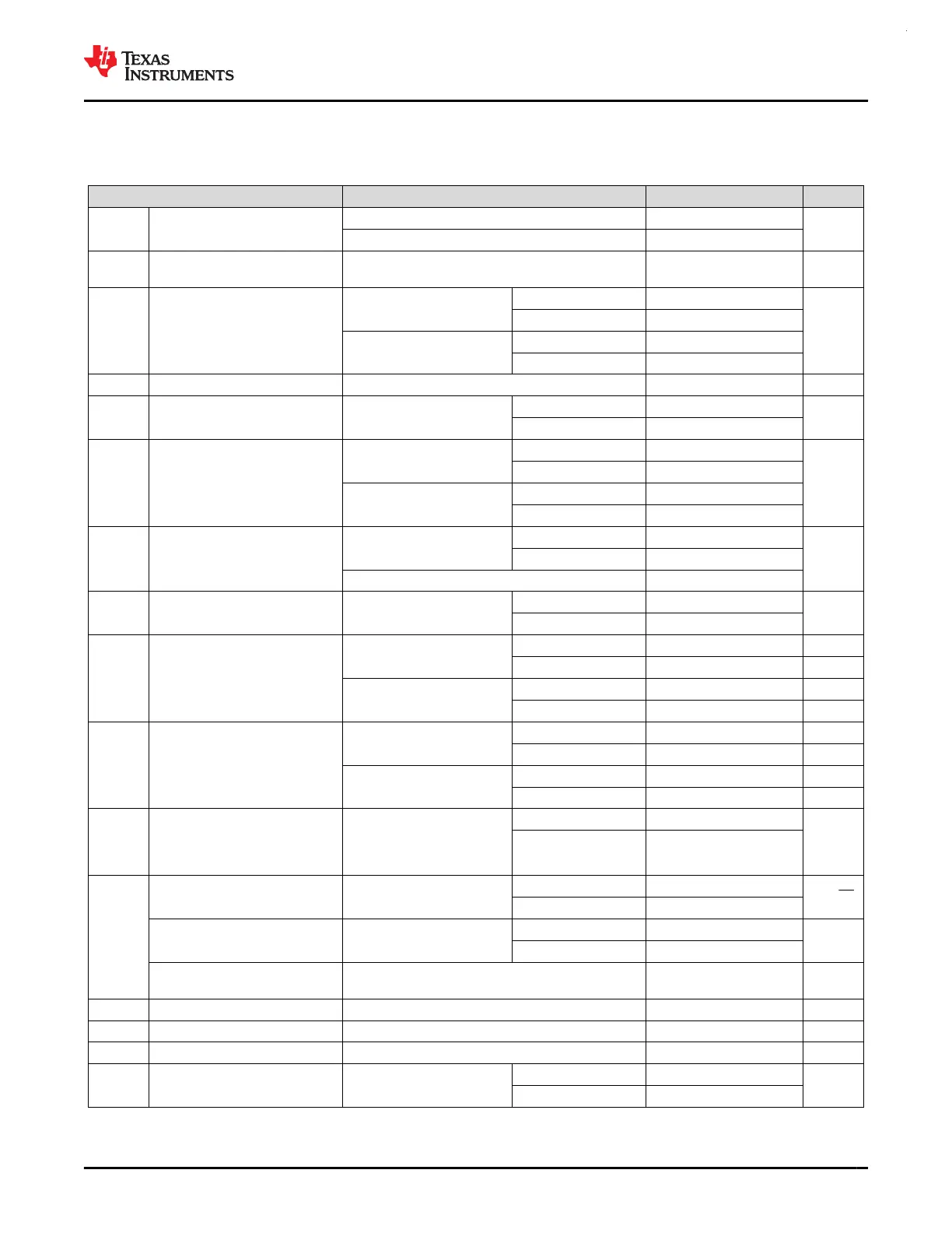
7.18 OPA
7.18.1 Electrical Characteristics
over recommended ranges of supply voltage and operating free-air temperature (unless otherwise noted)
PARAMETER TEST CONDITIONS MIN TYP MAX UNIT
V
CM
Common mode voltage range
RRI = 0x0 -0.1 VDD-1.1
V
RRI = 0x1 -0.1 VDD-0.3
V
O
Voltage output swing from rail
range
R
L
= 10kΩ connected to VDD/2 20 68 mV
I
q
Quiescent current, per op-amp
I
O
= 0mA, RRI = 0x0
GBW = 0x0 100
µA
GBW = 0x1 350
I
O
= 0mA, RRI = 0x1
GBW = 0x0 140 170
GBW = 0x1 450 600
I
BCS
Burn-out current source current 2 µA
GBW Gain-bandwidth product C
L
= 40 pF
GBW = 0x0 1.5
MHz
GBW = 0x1 6
V
OS
Input offset voltage
Noninverting, unity gain,
VDD = 3.3V, T
A
= 25°C
CHOP = 0x0 ±0.4 ±2
mV
CHOP = 0x1 ±0.3
Noninverting, unity gain,
VDD = 3.3V
CHOP = 0x0 ±1.5 ±3.5
CHOP = 0x1 ±0.1 ±0.5
dV
OS
/dT
Input offset voltage temperature
drift
Noninverting, unity gain,
CHOP = 0x0
GBW = 0x0 ±6
µV/°CGBW = 0x1 ±5.2
Noninverting, unity gain, CHOP = 0x1 ±0.5
PSRR
DC
Power Supply Rejection Ratio,
DC
Noninverting, unity gain
CHOP = 0x0 45 200
µV/V
CHOP = 0x1 40 200
I
bias
Input bias current
0.1V<V
in
<VDD-0.3V, VDD =
3.3V, CHOP=0x0
T
A
= 25°C ±50 pA
T
A
= 125°C ±0.35 ±100 nA
0.1V<V
in
<VDD-0.3V, VDD =
3.3V, CHOP=0x1
T
A
= 25°C ±0.4 nA
T
A
= 125°C ±0.4 ±104 nA
I
bias
Input bias current for dedicated
OPA input pin
0.1V<V
in
<VDD-0.3V, VDD =
3.3V, CHOP=0x0
T
A
= 25°C ±6 pA
T
A
= 125°C ±0.35 ±0.4 nA
0.1V<V
in
<VDD-0.3V, VDD =
3.3V, CHOP=0x1
T
A
= 25°C ±0.4 pA
T
A
= 125°C ±0.4 ±0.5 nA
CMRR
DC
Common mode rejection ratio,
DC
RRI = 0x0:
0V<V
CM
<VDD-1.1V
RRI = 0x1:
0V<V
CM
<VDD-0.3V
CHOP = 0x0 89
dB
CHOP = 0x1 or 0x2 73 102
e
n
Input voltage noise density
GBW = 0x0, Noninverting,
unity gain, CHOP = 0x0
f = 1kHz 240
nV/√Hz
f = 10kHz 88
Integrated voltage noise, input
referred
f = 0.1Hz to 10Hz, GBW =
0x0, Noninverting, unity gain
CHOP = 0x0 75
µVpp
CHOP = 0x1 or 0x2 2
Integrated voltage noise, output
referred
f = 0.1Hz to 10MHz, GBW = 0x0, CHOP = 0x0,
Noninverting, unity gain
1.5 mVpp
R
in
Input resistance
(1)
2.6 kΩ
C
in
Input capacitance Common mode 3 pF
A
OL
Open-loop voltage gain, DC R
L
= 20kΩ to GND, 0.3<Vo<VDD-0.3 93 dB
PM phase margin C
L
= 40pF
GBW = 0x0 57
degree
GBW = 0x1 48
www.ti.com
MSPM0G3507, MSPM0G3506, MSPM0G3505
SLASEX6A – FEBRUARY 2023 – REVISED JUNE 2023
Copyright © 2023 Texas Instruments Incorporated
Submit Document Feedback
45
Product Folder Links: MSPM0G3507 MSPM0G3506 MSPM0G3505
 Loading...


