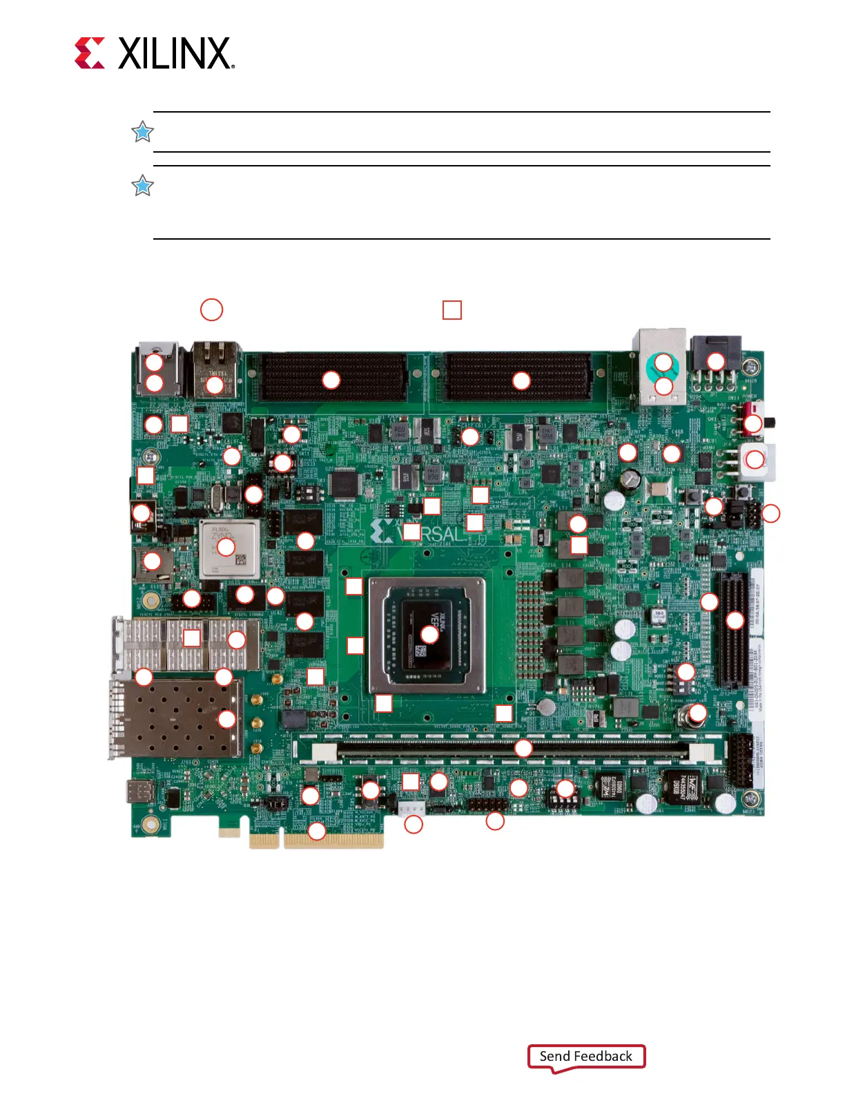
IMPORTANT! The following gure is for visual reference only and might not reect the current revision of
the board.
IMPORTANT! There could be mulple revisions of this board. The specic details concerning the
dierences between revisions are not captured in this document. This document is not intended to be a
reference design guide and the informaon herein should not be used as such. Always refer to the
schemac, layout, and XDC les of the specic VCK190 version of interest for such details.
Figure 3: Evaluation Board Component Locations
00
Round callout references a component
on the front side of the board
Square callout references a component
on the back side of the board
00
1
40
37
36
39
2
41
22
42
33
34
26
23
11
15
13
8 47
14
50
12
52
43
4
10
48
3
9
7
49
55
54
18
20
21
19
18
53
19
28
38
11
45
44
27
27
16
17
16
17
32
30
31
25
35
5
29
6
24
51
46
X24958-121420
Chapter 2: Board Setup and Configuration
UG1366 (v1.0) January 7, 2021 www.xilinx.com
VCK190 Board User Guide 14

 Loading...


