• Part number: MTA9ADF1G72AZ-3G2E1
• Descripon
○ 8 GB 288-pin DDR UDIMM
○ Single rank
○ 8 Gb (1 Gig x 8), 16 banks
○ Supports up to 3200 Mb/s
The VCK190 XCVC1902 ACAP DDR interface performance is documented in the Versal Prime
Series Data Sheet: DC and AC Switching Characteriscs (DS956). The VCK190 DDR4 DIMM
interface adheres to the constraints guidelines documented in the PCB guidelines for DDR4
secon of the Versal ACAP PCB Design User Guide (UG863). The DDR4 DIMM interface is a 40Ω
impedance implementaon. Other memory interface details are also available in the Versal ACAP
Memory Resources Architecture Manual (AM007). For more details, see the Micron
MTA9ADF1G72AZ-3GE1 data sheet at the Micron website. The ACAP connecons for the
feature described in this secon are documented in the VCK190 board XDC le, referenced in
Appendix B: Xilinx Design Constraints.
LPDDR4 Component Memory
[Figure 3, callout 3 and 4]
The VCK190 board hosts two LPDDR4 memory systems, each with a component conguraon
of 2x (1x32-bit component).
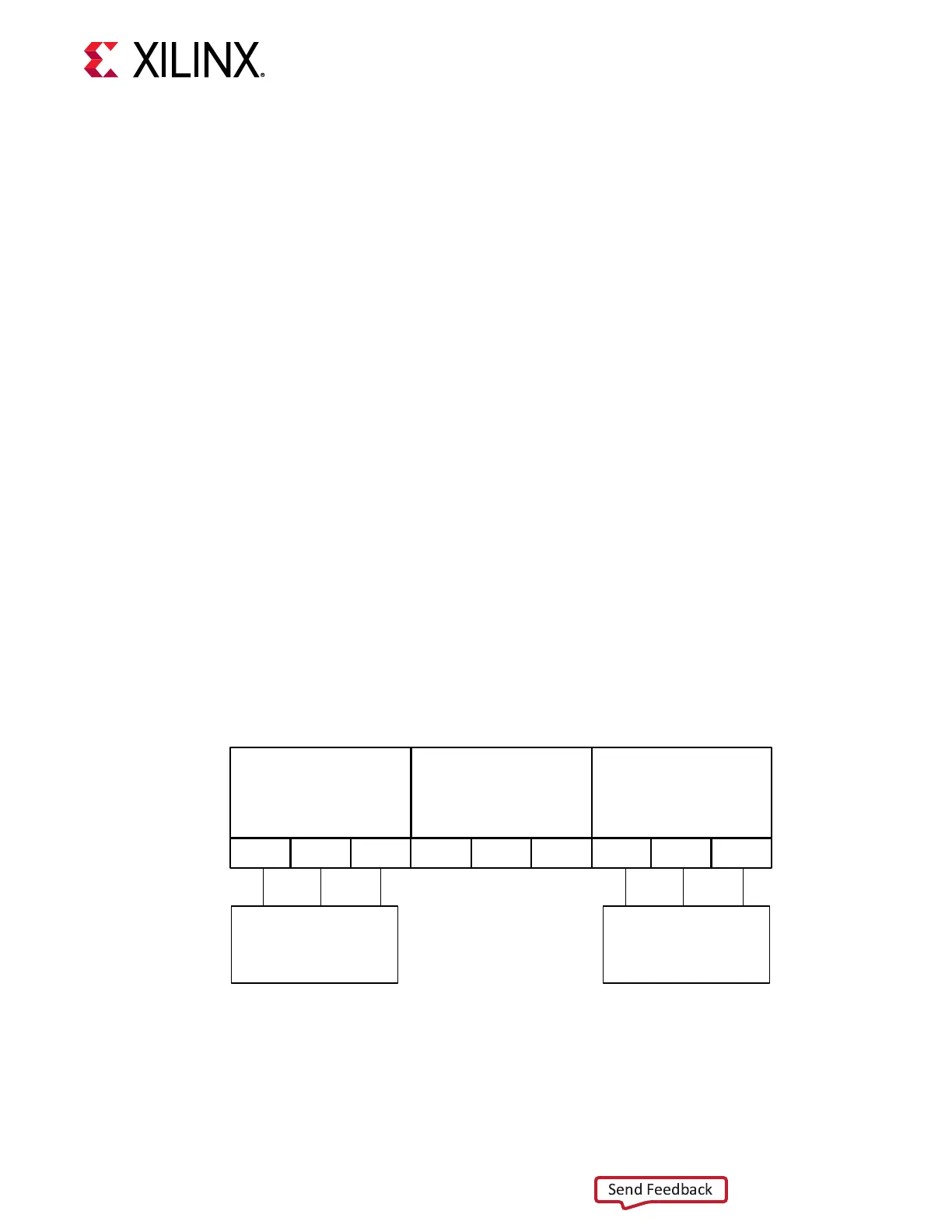
Figure 7: LPDDR4 Component Memory
XPIO
Triplet 2
XPIO
Triplet 3
XPIO
Triplet 4
703 704 705 706 707 708 709 710 711
LPDDR4
2x (1x32)
LPDDR4
2x (1x32)
X23198-090919
XCVC1902 U1 XPIO triplet 2 (banks 703/704/704) and triplet 4 (banks 709/710/711) each
support two independent 32-bit 2 GB component interfaces (4 GB per triplet).
• Manufacturer: Micron
Chapter 3: Board Component Descriptions
UG1366 (v1.0) January 7, 2021 www.xilinx.com
VCK190 Board User Guide 26

 Loading...


